The information on this page is based on evaluation of
an early prototype.
The information shows how the design was made, but actual
performance of the unit and the entire system will be uploaded
at the
main page for the RXHFA unit
when the first production batch is evaluated.
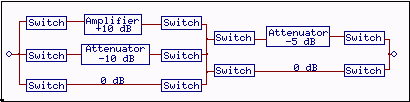
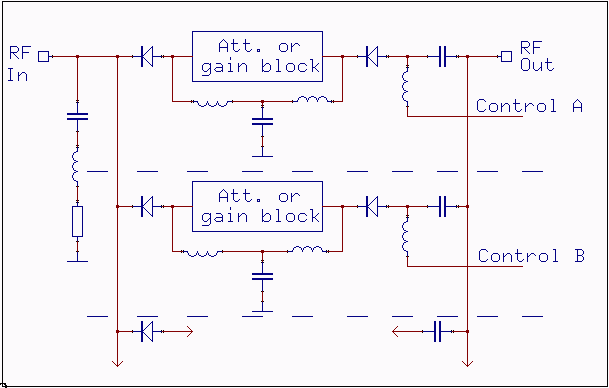
System gain and intermodulation characteristicsA hf receiver may be operated from a low efficiency antenna that does not produce much signal. In such situations a low noise figure is needed. A good receiver needs a dynamic range of about 100dB according to a study by Peter E. Chadwick, G3RZP HF Receiver dynamic Range: How Much Do We Need? which appeared in the May/June 2002 issue of QEX. The problem is that the third order intercept point has to be +33 dBm according to this study and that can not easily be combined with a low noise figure. It is not necessary however. At times when IP3 has to be around 30 dB, it is ok for the noise figure to be relatively high.Switches are used to switch in and out attenuators and amplifiers in order to shift the noise floor and the point of saturation up or down to fit the demands of the situation. A 10 dB attenuator will degrade the noise figure by 10 dB but it will also shift IP3 10 dB upwards for an unchanged dynamic range. The RXHFA uses the block diagram shown in figure 1. |
|
|
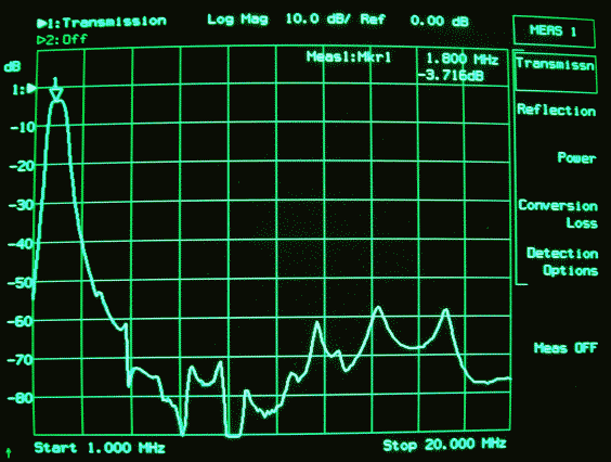
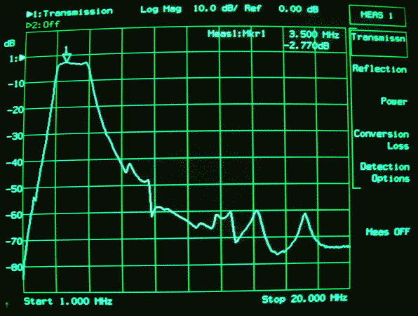
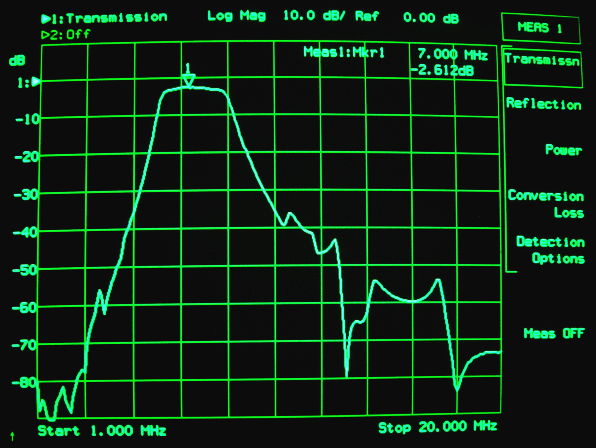
Fig 1. Block diagram for system gain setting in the RXHFA converter. Without any RF filters, the RXHFA unit has the intermodulation performance listed in table 1. The measurements were made on 14 MHz. At a level setting of -10 dB, the system noise figure is 30 dB and IP3 is +37 dBm. This is well in line with the requirements given by Peter E. Chadwick. The noise floor is at -144 dBm/Hz which corresponds to -121 dBm in a 200 Hz wide CW filter. For a third order intermodulation product to be of similar level, two interfering signals have to be at -16 dBm. For a second order intermodulation product to reach -121 dBm, it is sufficient if two interfering signals are at -33 dBm. The IP2 of +55 dBm is not quite good enough. there may be plenty of signals around 7 MHz that much stronger than this and that may cause harmful interference. Table 1Intercept points at different gain settings for the RXHFA unit on 14 MHz without any RF filter. The noise figure is an estimated system noise figure. The RF filtersTo remove second order intermodulation and also to limit the peak voltage seen by amplifiers and mixers, band pass filters are placed in front of the gain setting block. These filters remove the second order intermodulation, but they do introduce some third order intermodulation at low system gain settings. The filters introduce about 3 dB attenuation. The intermodulation performance of the RXHFA unit on 14 MHz with the filter in place, but with the RF switches replaced by wires is shown in table 2. IP3 degrades with frequency because the standard inductors from TDK does not contain sufficient amounts of ferrite. On 1.8 MHz IP3 of the input filter is about +36 dBm, on 3.5 and higher bands IP3 is above +40 dBm, I do not have notch filters for all bands so I do not know precisely. In case better than +36 dBm is needed on 1.8 MHz one can easily put an attenuator in front of the RXHFA unit and set the internal gain of the unit correspondingly higher. In other words, do not set the level below -5 dB on 1.8 MHz in case there is a need for better than +35 dBm IP3.Table 2 Intercept points at different gain settings for the RXHFA unit on 14 MHz with RF filter but without a switch in front of the filter. The noise figure is an estimated system noise figure. Frequency responses are shown in figures 2 to 6. A network analyzer is connected to the antenna input, all output switches are set in the off state and the network analyzer is connected to the common output of the filter bank. The input standing wave ratio is typically 1.5 on all bands. |
|
Fig 2. Frequency response of the filter bank when set for 1.8 MHz. |
|
Fig 3. Frequency response of the filter bank when set for 3.5 MHz. |
|
Fig 4. Frequency response of the filter bank when set for 7 MHz. |

|
Fig 5. Frequency response of the filter bank when set for 10 MHz. |

|
Fig 6. Frequency response of the filter bank when set for 14 MHz. RF switchesThe signal path contains six switches after one another. This means that the insertion loss has to to be low, otherwise there would be a need for a second RF amplifier.A CMOS switch like the 74HC4053 has a typical on resistance of 45 ohms with a maximum value of 135 ohms according to the data sheet. In a 50 ohm system, such a switch gives an attenuation of 3 dB (or more). A transistor like the J108 with a channel resistance of less than 8 ohms will have a loss in the order of 0.4 dB and could be used. I have not tried the J108, but the J105 which has a channel resistance of 3 ohms provides excellent intermodulation characteristics but the isolation in the off state is poor, only 17 dB, because of the high capacitances. The J108 could be expected to provide 23 dB isolation because the data sheet indicates that the capacitances are approximately a factor of two smaller. A J310 gives an isolation of about 34 dB but the insertion loss is nearly 2 dB. Four J310 in parallel would provide 0.5 dB loss and 22 dB isolation and should be equivalent to a single J108. An alternative to the FET switch is the diode switch. An ordinary diode such as the 1N4148 can be used as an RF switch with low distortion as long as the current through the diode does not vary noticeably over the RF cycle. For use in receiver front ends we might want to allow power levels (1 dB saturation) in the order of +20 dBm which means that the RF current in a 50 ohm system is about 45 mA RMS or 63 mA peak. To allow such signals the DC current through the diode has to be about 100mA with a variation from 37 to 163 mA. Figure 7 shows the switching arrangement used in the RXHFA unit for switching in RF amplifiers or attenuators. The control voltage is set at +5V for the desired functional block while the control voltage is set to -5V for all other blocks. |
|
Fig 7. Schematic diagram for the diode switches used in the RXHFA converter. By using PIN diodes rather than ordinary diodes, one can operate the diode switch at a much lower current. The diode switches, like everything else is a source of intermodulation. Figure 8 shows the IM3 performance of the diode switch at different currents both with fast diodes and with PIN diodes used as the switching element. PIN diodes are not easily available, the base-collector diode of a transistor can be used instead. The data is from 1.6 MHz, the advantage of the PIN diode decreases with frequency and 1.6 MHz is close to the lowest frequency of operation for the RXHFA unit. (It happens to be a frequency for which the junk box could provide the crystal for a notch filter) It is immediately obvious from the figure that the transistor diode needs much less current to provide low enough third order intermodulation. |
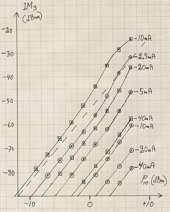
|
Fig 8. Third order intermodulation characteristics for one block with two diodes according to figure 7 with diode current as parameter. Boxes are with 1N4148 as the switching element, circles are with the base-collector diode of old BC547B transistors. The frequency is 1.6 MHz. The third order intercept points change with diode current as shown in table 3. At 40 mA the transistor is 10 dB better than the diode and the difference is larger at lower currents. The frequency of the measurements is 1.6 MHz, the difference is larger at higher frequencies because the carrier lifetime that causes the difference will be more significant. Table 3 Third order intercept point of a switch with a single diode at 1.6 MHz. The development in semiconductor technology goes towards smaller structures and less silicon. The data of figure 8 and table 3 were obtained with BC547B devices from the junk box. When buying new devices in December 2003, one gets a slightly "better" transistor which means that it is not quite as good to use as a PIN diode. Table 4 shows the performance of a single diode of various types operated as a switch with a forward current in the on state of 20 mA and with a reverse bias of 5V in the off state. |
Table 4 Third order intercept point, isolation and insertion loss for a single diode operated as switch with 20mA DC current. |
On the basis of table 4 one would like to use the BAQ800 AM PIN diode,
but that would be a mistake for the first group of diodes at the antenna
input.
Diodes have a capacitance that varies with the voltage.
Because of that, they generate second order intermodulation.
The front end of the RXHFA unit uses five filters so there are
four diodes that produce second order intermodulation.
Table 5 gives the level of second order intermodulation with
different diodes used for the four off-state switches with a wire
replacing the on-state diode.
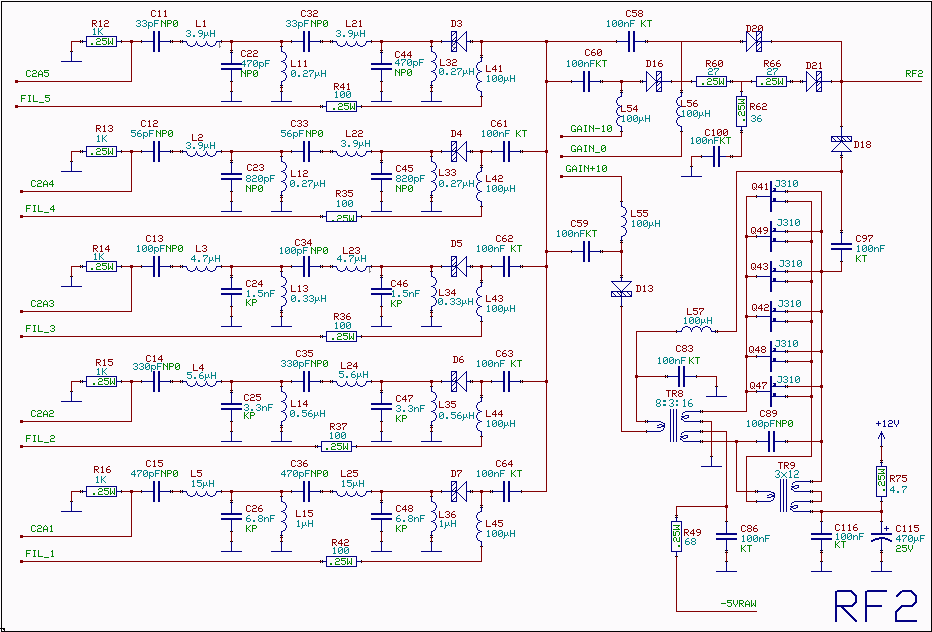
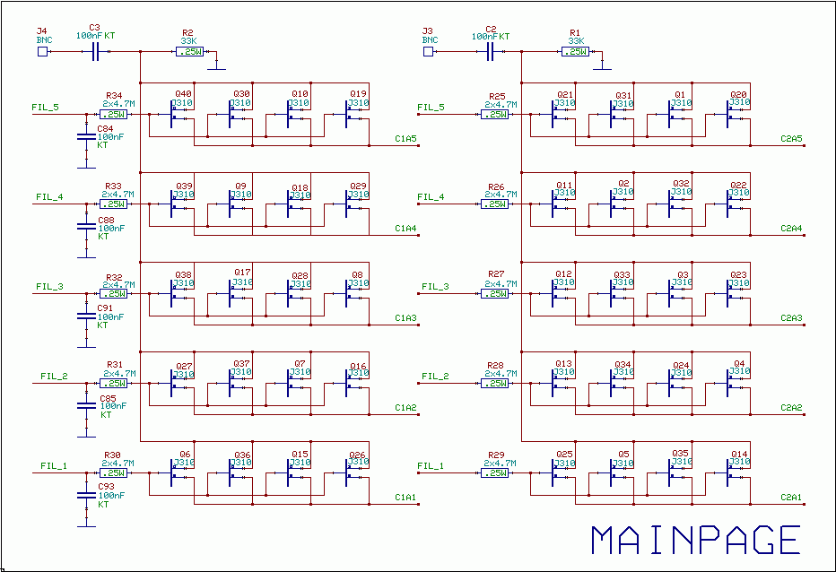
Table 5 Second order intercept point for the RXHFA input selection switch with the on-state diode replaced by a wire and with four identical diodes for the off-state. An inspection of tables 4 and 5 shows that the base-collector diode of BF240 transistors would be a reasonable choice for the input switch and provide something like IP2=73 dBm and IP3=44 dBm at a current of about 50mA. The RXHFA has two channels so the current needed for the input switch will be larger than conveniently supplied from a 74HC4053. To avoid this problem and to reduce the number of inductors needed, the input switch is four J310 in parallel. This gives IP2 = +82dBm. IP2 drops rapidly if fewer transistors are used. As an alternative a single J108 could be used, but that would require a larger voltage swing for the control voltage so the total complexity would not differ much. The control voltages are set by the computer through a simple serial interface The schematic diagramFigures 9 to 11 show the complete schematic diagram of the input section with filters, amplifiers, attenuators and switches. Note that the diodes with hatched cathode are symbols for the base-collector diode of BC547B transistors. |

|
Fig 9. The RXHFA front end for channel 1. |
|
Fig 10. The RXHFA front end for channel 2. |
|
Fig 11. The RXHFA input switches. |