A series resonance X-tal oscillatorThe oscillator is similar to the oscillator used for conversion from 10.7 to 2.5 MHz. but there is no frequency divider at the output. The RXHFA uses transformer coupled stages to allow a larger bandwidth in the feedback amplifier and one series resonance circuit for each crystal to pick the correct overtone for oscillation. The schematic diagram is given in fig. 1.An oscillator can be seen as an amplifier which has feedback through a filter. The amplifier of a series resonance oscillator must have both a low input impedance and a low output impedance, preferrably well below the series resonance impedance of the X-tal, to preserve the selectivity associated with the high Q of the X-tal itself.
|

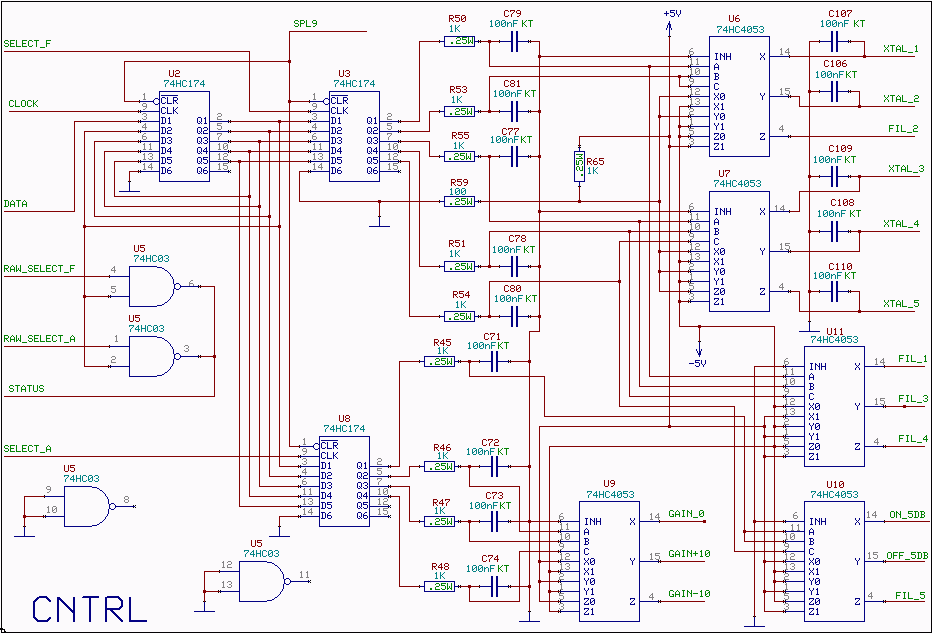
Functional description.The oscillator amplifier has five input transistors MPSH10. Only one of these transistors is active with its control voltage XTAL_1 to XTAL_5 held at -5V. The other control voltages are kept at +0.5V.Assume XTAL_1 = -5 V. Then the current in Q61 becomes about 10 mA, it is set by R69 over which the voltage is about 4.3 V. The emitter is protected from the thermal noise in R69 by the parallel resonance of C134 and L74. C74 also serves the purpose of loading the emitter with 470 ohms at UHF frequencies where oscillations otherwise might occur. The inductor L78 forms a series resonator with C147. By tuning C147 slightly out of resonance, the frequency can be adjusted. L78 also isolates the emitter from the large capacitance of the crystal. This helps to avoid oscillations at VHF/UHF frequencies where the transistor works as an emitter follower with the emitter loaded by 470 ohms only. L81 balances the parallel capacitance of the crystal and makes the impedance seen by the emitter very high at the sides of the series resonance, thereby providing very low gain and very low noise at the output of Q61 at frequencies well away from the resonance. This allows the sideband noise to be well below the thermal noise of the crystal, something which is not possible with a small resistor from the emitter to ground. At the drain side, Q61 is loaded by the capacitances of the collector base capacitances of the other four input transistors, C132, R90 and R92 give some negative feedback at VHF and UHF frequencies while the small resistance of R92 makes the base grounded at and near the frequency of oscillation. The small amount of thermal noise generated in R92 does not add sideband noise, it is not amplified because of the high impedance at the emitter. Q61 is loaded by a low impedance. TR1 is wound on a low loss toroid, it is 14 turns in total and the tap is 6 turns from ground. The inductance of TR1 balances the stray capacitances making the impedance seen by the source of Q83 several hundred ohms over the frequency range 56 to 69 MHz. The transformation ratio is 14 to 6 which means that the RF current through Q83 is only about 2 times larger than the RF current in Q61. Because of the high source impedance Q83 gives low gain and very little noise. If TR1 were replaced by a ferrite core of the same type used for the other transformers, the losses of the ferrite would add significant amounts of noise at the input of Q83 causing about two dB higher sideband noise levels. The fact that the about 50 ohms input impedance of Q83 loads TR1 much more than the losses does not mean that the losses are harmless. By disconnecting the crystal and L81, then injecting a very weak signal into the emitter through a small capacitor one can study the performance of the LO feedback amplifier and make sure that the very weak noise from Q61 dominates over the noise from Q83 at the Q83 output. Likewise it is possible to make sure that Q66/Q84 do not degrade the noise performance of the LO amplifier. As it turns out, the higher signal level makes it possible to run the source at a lower impedance and to use ferrite beads for TR2. With a 3 to 1 transformation ratio the impedance transformation is 9 to 1 and it is not possible to do such a transformation over a wide bandwidth using a low loss toroid. The DC current through Q66/Q84 is about 40 mA, these transistors saturate and set the level of oscillation. The output of Q66/Q84 is loaded by 120 ohms, 25 times the 4.7 ohms of R119 because the transformer TR3 has a 5:1 transformation ratio. Q66/Q84 are also loaded by R115 through the series resonance of L91 and C182. The series resonators for the other crystals also load Q83 and Q84 slightly, but they are off resonance so they do not load much. The voltage across R115 is fed into Q61 through the crystal closing the loop to provide oscillations. The sideband noise at a frequency separation of 100 kHz is about -167 dBc/Hz for the entire WSE converter system. This is about 4 dB worse than the sideband noise of the system sideband noise without the RXHFA unit. The RX70 unit uses a resonant circuit for impedance transformation in the LO feedback oscillator and givs less than 50% of the total sideband noise. Computer interfaceThe oscillator frequency and the front end gain levels are selected by a simple low speed serial interface that is adopted for all WSE Linrad hardware. Each unit has four communication pin's:
Select(input)
These pins are intended to be connected directly to the parallel port of the PC for small systems, one separate data pin for each select input with all the other pin's in parallel. Larger systems need a decoder to convert 6 pin's to one of 64 pin's. The RXHFA box is two logical units, one for setting the frequency and another for setting the system gain. The control lines are are well decoupled to avoid sending interference into the oscillator or front end. The user program is responsible for setting the d-type flip-flops right so only one of the 74HC4053 outputs is at minus 5 volts while the other four are at plus 5 volts for the oscillator selection. Likewise the user program has to set only one of the five control lines for the input filter bank high and one of the three control lines for the 10 dB gain stepping high.
|