
Fig. 1. Top view.
|
The main article is
here
|
|
Fig. 1. Top view. |
|
This oscillator is an experiment that I made to improve my own understanding of sideband noise in oscillators. The phase noise is similar to the best oscillators by Wenzel Associates, Inc which are claimed to be the best in the industry with phase noise down to -180dBc/Hz at 20 kHz. This unit is equipped with the cheapest possible standard crystals. They are overtone crystals designed for 42.5 MHz. This unit is not optimized for power consumption, cost or any other normal design target. It is just an experiment to satisfy my personal curiosity and to (perhaps) give ideas about how to design really good VHF oscillators at about 10 times higher frequencies. The unit contains power-hungry class A amplifiers with noiseless feedback so the power consumption is high: 7 W (0.47A at 15 V) To keep a reasonable temperature there is a large heat sink in copper which is in thermal contact with the 7812 voltage regulator and the two BUK75150 power MOS-FETs that are used for the class A amplifiers. |

Fig 2. View from below with the lid off. |
|
The view from below is shown in figure 2. The unit is in a birds nest style so the oscillator is a little more microphonic than a "proper" construction would be. |

Fig 3. |
|
The block diagram is straightforward. An amplifier followed by an amplitude limiter with feedback through a crystal filter. There is also a buffer stage to isolate the output. The buffer uses noiseless feedback so the load impedance will affect the input impedance. The attenuator is inserted to reduce the effect of impedance variations at the output. |

Fig 4. |
|
The crystal filter is a two crystal ladder filter. When running the unit as an oscillator there is presumably no advantage in the extra stop band attenuation provided by using two crystals rather than one. There is no disadvantage either, but the ladder filter makes it possible to investigate the noise properties that the unit would show as an oscillator by using it as an amplifier with a standard signal generator rather than feedback to generate an oscillation at the peak of the crystal filter. Two crystals are then needed considering the sideband noise of available signal generators. The components enclosed in red are inserted to avoid spurious oscillations. At 1 MHz the filter would be a T link with two 15 uH inductors and a 2.2nF capacitor with almost no loss. That resonance is killed with a 10 ohm resistor across the 2.2 nF capacitor. At 14 MHz this 10 ohm resistor has no effect because of the 0.47 uH inductor in series with it. Oscillations that originally occured at 1 MHz were stopped this way. In the final design they would not occur because by series tuning the input for a resistive 50 ohm load rather than tuning it with a parallel capacitor (at another number of turns) the 1 MHz resonance is killed. That means that the 10 ohms 4.7 uH link is not needed any more, but it makes no harm. The purpose of the inductors across the crystals is to balance the parasitic capacitance across the crystal. |

Fig 5. Note that the emitter inductor is 22 uH, there is a drawing error in the figure. The 22 uH inductor has its self-resonance at 14 MHz with an impedance of about 10 k ohm. |
|
The details of the input amplifier and limiter.
The 2.2 uH inductor at the emitters balances the stray capacitances
to ground and makes the impedance as high as possible
at the emitter.
Three bipolar transistors MPSH10 are connected in parallel.
The DC current through each transistors is 18 mA.
The RF current through the emitters and also through the second
crystal is 8.8 mA which means that the power dissipation in the
crystal is about 0.6 mW.
The current through the first crystal is 14.5 mA which means that
it is heated by 1.7 mW and that would probably be too much in
the long run.
It is not any problem for an experimental unit like this one
which is likely to not run many hundred hours during its
entire life.
A proper design based on the experiences with this unit would
only use the second crystal at about .5 mW power dissipation.
|

Fig 6. |
|
The buffer has low Q band pass filters on both input and output. The second harmonic is 45 dB below the fundamental in the output signal. The +12V supply is carefully decoupled like this: |

Fig 7. |
|
Note that the 3300 uF capacitor makes a small but clearly visible difference to the sideband noise at 10 kHz. This is despite the fact that there is a low pass filter from this +12V supply to each amplifier. When the unit is run as an amplifier with a dummy load at the input and with a 50 ohm low noise amplifier at the feedback output the spectrum below is obtained. |

Fig 8. |
|
The system noise figure at the low noise amplifier input is 3.5 dB. It means that the noise generated by the low noise amplifier and the rest of the test system (another amplifier followed by a Perseus) has to be 1.24 times larger than 290 K for a total noise temperature of (290 + 1.24*290) K when a room temperature dummy load is connected. That is the zero point of the dB scale. 650 K. Well away from the center frequency the measured noise level at the feedback output is 3 dB corresponding to 1300 K. That means that the noise temperature of the feedback output well away from the center is 650 K corresponding to -170.5 dBm/Hz. On the center frequency the noise is 17.7 dB on the scale which means that the noise temperature is 58.9 * 650 =38285 K All but 650 K originates in the unit under test for which the power density at the center frequency becomes -152.9 dBm/Hz on the feedback output. The small signal gain and frequency response from the filter input to the feedback output can be found from this network analyzer output: |

Fig 9. |
|
The small signal gain is 3.2 dB. The noise figure at the filter input is 18 dB. With L = Power loss through the filter and G = power gain from filter to feedback output the following equations can be set up: NFin = 18 = NFamp + L NFamp = 174-152.8 -G G - L = 3.2 The numbers are accidentally in perfect agreement. The uncertainty in a difference between two noise figure measurements which is what is behind the equations is in the order of 0.3 dB. The power level required on the input to drive the amplifier to its normal level is 6.5 dBm. That is the power required to produce 0.5 mW power in the crystal. The filter output impedance is 10 ohms while the input impedance of the amplifier is 4 ohms. That means that only -6 dBm is delivered to the transistors while the second crystal with its 8 ohm resistance absorbs twice as much power. The attenuation from the input connector to the transistor L is thus 12.5 dB which means that the noise figure is 5.5 dB which is reasonable considering the mismatch with VSWR=2. The gain of the transistor is thus 15.7 dB which means that the current feedback of the second stage loads the collector side with about 150 ohms. With -6 dBm power delivered to a transistor with NF = 4.5 dB the sideband noise would have a lower limit at -163.5 dBc/Hz. At "large" frequency separations (above 1 kHz) this oscillator could be perhaps 17 dB better, 180.5 dBc/Hz and since only 50% of the noise is phase noise the lower limit for phase noise performance should be somewhere around -183.5 dBc/Hz. The small signal gain from the filter input to the buffered output is 13.2 dB as can be seen here: |

Fig 10. |
|
The filter peak is too narrow to come out correctly when the network analyzer is swept over 100 kHz, but one can see that the attenuation is better than 68 dB at a frequency separation of 10 kHz: |
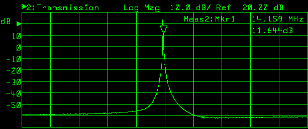
Fig 11. |
|
This is good enough to allow investigations by use of e.g. a HP8657A signal generator. The noise one can observe 10 kHz from the center will not be leakage through the filter of the generator sideband noise but noise created internally in the unit. The spectrum at the buffered output should be 10 dB above the spectrum at the feedback output. When measured in exactly the same way as the feedback output this is the result: |

Fig 12. |
|
The peak is 10.3 dB above the peak at the feedback output while the noise floor is only about 7.4 dB above the noise floor at the feedback output. The reason is that the noise of the of the test system is negligible at the buffered output while it contributes nearly 50 % of the noise at the feedback output. Since the zero point of the dB scale corresponds to the test system, 650 K, the noise floor 11.4 dB above zero corresponds to 8970 K out of which 650 K is the test system. The power density of the noise generated by the unit is thus 14.4 dB above -174 dBm/Hz or -159.6 dBm/Hz. The output power vs input power at the two outputs is shown below. Both outputs are terminated in 50 ohms for this measurement. |

Fig 13. |
|
Since the small signal gain is 3.2 dB oscillations should occur at a level where 3.2 dB gain is lost at the limiter output. At that point 0.8 dB gain is lost at the buffered output. The gain loss at the buffered output is due to onset of saturation in the MPSH10 transistors. To study by how much the noise floor 10 and 20 kHz away from the center frequency increases when the power level increases the following test configuration was used: 1) Signal generator HP8657A 2) Unit under test 3) Attenuator -3 dB 4) Matchbox 5) Crystal notch filter 6) Low noise amplifier 7) LC notch filter 8) 6 dB amplifier 9) 6 dB amplifier 10) Perseus 11) Linrad Linrad was set to show 0 dB when a dummy load was connected to replace the test object. The results are shown here: |

Fig 14. |
                Measured at    Measured at      Test object     Test object
Offset   NF     P = 0 dBm      P = 6.5 dBm       P = 0 dBm      P = 6.5 dBm
 (kHz)  (dB)   (dB) (lin)       (dB) (lin)      (lin) (dB)     (lin) (dB)
  10    11.0    5.0  3.16       6.2   4.17       2.16 3.3       3.17 5.0
  20     9.0    6.5  4.47       7.2   5.25       3.47 5.4       4.25 6.3
The noise is exactly the same when the unit runs as an oscillator with an output power of 18.5 dBm corresponding to an input level of 6.5 dBm as when it runs with the HP8657A set to deliver 6.5 dBm From this measurement the noise floor at 10 kHz is -174+11+3.3 dBm/Hz = 159.7 dBm/Hz when no signal is present while it is 159.6 at 20 kHz. This is in excellent agreement with the previous independent measurement. At a power level of 6.5 dBm the noise is a little higher, -158.0 dBm/Hz = -176.5 dBc/Hz at 10 kHz and -158.7 dBm/Hz = -177.2 dBc/Hz at 20 kHz. Most of the noise is independent of the signal level so it is reasonable to assume 50% is amplitude noise and 50% is phase noise. That means that this unit should have a phase noise of -179.5 dBc/Hz @ 10kHz and 180.2 dBc/Hz @ 20 kHz By changing the limiter it is possible to increase the power level. For an output power of 22.2 dBm with +3dBm power developed in the crystal the noise at 20 kHz would be at 157.8 dBm/Hz or -180 dBm/Hz with a phase noise of -183 dBc/Hz @20 kHz I do not know for how long a crystal can tolerate +3 dBm of power dissipation. The purpose of this investigation is not to design oscillators that outperform the best commercially available ones but to understand what factors are important. I am not aware of any application in which better than -180 dBc/Hz would be of any interest for an oscillator in the HF range. The experiences from this investigation should however be applicable to VHF crystal oscillators where very low phase noise might be of interest. When I first made the measurement of sideband noise vs generator level the noise increased by about 10 dB from zero to 6.5 dBm. That noise was not quite calm, it had occasional bursts of a little stronger noise that indicated some kind of poor connection. This noise disappeared when I replaced all carbon film resistors with metal film resistore. It is interesting to note that a large capacitor across the source resistors of the MOSFETs increases the sideband modulation by several dB. Reducing the current through the MOSFET increases the sideband noise and makes the effect of a big capacitor on the source larger. The conclusion is that the BUK75150 transistor produces modulation when there is a small component of audio current through the transistor. Using a small capacitor like 0.15 uF will decouple 14 MHz but leave the audio impedance at the level set by the source resistor. By connecting an audio signal to the base and thereby forcing a known audio current through the transistor I could determine the percentage of audio current needed to produce modulation sidebands 50 dB below the main signal.
     3*MPSH10      47%
First BUK75150     10%
Second BUK75150     6%
The modulation in the MOS-FETS is both amplitude and phase modulation
while the MPSH10 that are 18 dB less sensitive as modulators produce
mainly AM modulation.
It was obviously a mistake to use the noiseless feedback low gain amplifiers with MOS FETs!!! After replacing the FETs with six parallel MPSP10 each and changing the output transformers for twice the voltage swing on the collectors by having the collector winding twice as many turns as the emitter winding and shorting the second 22 ohm resistor in the attenuator the output power has increased to +24.6 dBm with the same power through the crystal filter. The noise floor at the buffer output with dummy loads on the feed back input and output is -153.1 dBm/Hz which sets the lower limit of the sideband noise at -177.7 dBc/Hz. At a frequency separation of 20 kHz the noise increases by 0.2 dB when the feedback is connected and the output power becomes 24.6 dBm. At 10 kHz the noise increase is 0.8 dB. At 30 kHz and above the noise floor is totally independent of whether the output power is zero or +24.6 dBm. Assuming equal amounts of amplitude and phase modulation the modified unit performs like this. Separation Phase noise (kHz) (dBc/Hz) 10 -179.9 20 -180.5 50 -180.7 To SM 5 BSZ Main Page |