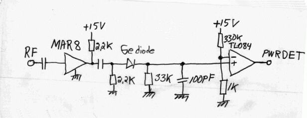
Fig 1. The power detector.
Tx control in SDR systems.It is of course possible to use a conventional sequencer in order to engage antenna relays and other relays that control DC voltages that disable power amplifiers. The purpose of this page is to show the solution I have adopted for fast Rx/Tx switching at high power levels with the purpose of using an SDR as a radar with a bandwidth compatible to a normal SSB signal.At the speed needed for a radar it is not possible to use any relays so all switching is electronic. That in itself is no complication and a conventional sequencer could be used to control the switching voltages if desired. As radio amateurs we use SDRs implemented in standard computers running a general purpose operating system like Windows or Linux. This creates timing problems since the computers are not deterministic. It is not possible to use the computer directly to control the sequence of the voltages needed for transmit/receive control. the time jitter would become too large. There are two aspects to worry about. One is that the antenna switch, a PIN diode, must always be set to the transmit state at least 0.5 ms before there is more than about 0.5W of transmit power and it must stay in the transmit state until the power has decreased below about 0.5W in order to not destroy the preamplifier or the PIN switch The other aspect is that the PIN switch should not be operated at power levels above about -50 dBm in order to not produce keying clicks that could cause interference to fellow amateurs. The pilot tone.The signal itself, whether it is Morse coded CW, SSB or something else is generated in the computer with a very precise timing as a digital signal. This digital signal can be clocked out through a soundcard in analog form or sent via ethernet, USB or whatever to an external A/D converter. In all cases, filters must be applied since a D/A converter will always generate alias signals above the Nyquist frequency. It is possible to send a weak signal at the Nyquist frequency to use as a control signal for TR switching without generating any false signals because the filters that are needed anyway will not let the signal through. An extra filter at the Nyquist frequency with a bandwidth in the order of 5 kHz will allow the detection of the pilot tone with a precise timing in relation to the waveform generated by the computer.The power detector.Computers are not 100% reliable. The SDR program itself could cause a crasch due to a program bug. Some other program could overload the processor(s) causing various errors in the generated waveform. It would be too hazardous to rely on the computer for the survival of the PIN diode switch and the antenna preamplifier. By use of an amplitude detector at a very low power level in the signal path it is possible to sense whenever the level is high enough for the output power to be too high for having the PIN diode switch in the Rx position with the all amplifiers in the transmit chain enabled. From this signal one can derive a control voltage for the PIN diode that starts immediately and that lasts some time after the signal is below a safe level. One can also derive a control signal for the transmit amplifiers that starts with a suitable delay and ends immediately as the signal goes below its threshold. This way the PIN diode is always operated well before and well after the transmit amplifiers provide amplification. It would be possible to use the amplitude detector as the only means for controlling the TR switch, but it would not allow perfect keying because the PIN switch would switch abruptly at the threshold power level in case the user produces waveforms that change slowly with time. By combining a power detector with a pilot tone detector one can have perfect keying with good reliability.A practical solution for TR switching.The details shown below are not intended to be copied in detail. I have used OP-amps and diodes for logic functions rather than CMOS or TTL logics because I have made just a single unit with the rats-nest style of building. There is a need for amplifiers as well as OR gates and something to generate time delays. Mounting ICs is far more work than mounting a couple of diodes and resistors in the rats-nest building style, that is why the details are as shown below. The logics is straightforward and could easily be implemented in standard ICs.The power detector, a simple amplitude detector is shown in figure 1. It is fed with an IF of the transmit signal, 10.7 MHz, to allow the same power detector to be used for all amateur bands. There are isolation amplifiers in front of the power detector to prevent the intermodulation generated by the MAR8 to reach the transmit path. Since the power detector should indicate "power on" at a signal level in the order of 40 dB below full power the MAR8 goes heavily into saturation at full power. |
|
Fig 1. The power detector. |
|
The pilot tone detector is an AM detector at 48 kHz and
like the power detector it also uses an OP-amp on its output
for logical levels -Vcc and +Vcc.
Figure 2 shows the sequencer. The output from the power detector and from the pilot tone detector are both delayed by about 0.5 ms in delay circuits. A delay circuit is shown in figure 3. The figure shows a delay(+) building block. It delays a positive transition by about 0.5 ms but it does not delay negative transitions. A delay(-) block is identical except that the two diodes are turned the opposite direction and it therefore delays negative transitions but not positive ones. The transmit amplifier is in the on state either by command from the power detector or from the pilot tone detector (or both). For both detectors, turning on the driver amplifiers is delayed, but turning off is immediate. The PIN diode switch is turned into transmit mode immediately but switching it to the Rx mode is delayed to happen about 0.5 ms after the driver amplifiers are turned off in case command is from the power detector. When the PIN diode is commanded by the pilot tone, there is no delay on the switching from Tx to Rx, the pilot tone detector itself has a time constant due to the filters used to improve the S/N of the pilot tone. |

Fig 2. The sequencer. |
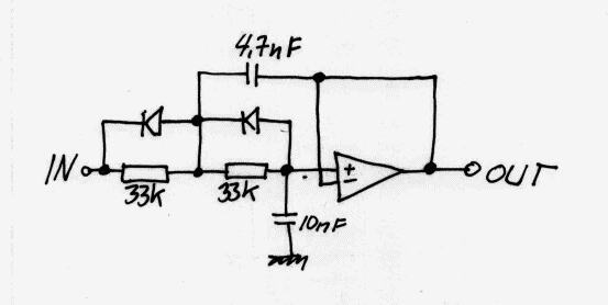
Fig 3. The delay(+) circuit. |
Switching waveforms.Figure 4 shows the operation of the sequencer under normal conditions and under simulated underrun errors. In this particular figure the time delay from key closure (upper trace) to full power output (lower trace) is 8 ms but there is time jitter on the time delay so it varies from about 6 to about 10 ms.The PIN diode is commanded to Tx mode by the sync tone well before the power starts to ramp up. The driver amplifier is turned on about 0.5 ms later which is also before power starts to rise. The amount of time by which these transitions should go before the power ramps up is set by the "pilot tone prestart" parameter. Both the PIN diode and the driver amplifier are switched off at the same time at the end of the key-down period. During the key-down interval an underrun error is simulated by clearing the data to the D/A converter during 0.8 ms. Here the RF and the pilot tone disappear abruptly. The switching is delayed like after a normal key up and that would happen even without a sequencer using the pilot tone only. When the output abruptly starts again, the PIN diode is switched immediately but the driver amplifiers are turned on with a delay. This will protect the receiver and antenna relay from excessive power. Figure 5 is identical to figure 4 except that the cable from the pilot tone detector is unplugged. One can see that the front end is well protected but that the driver amplifiers will do the actual keying and therefore produce keying clicks at each key-down. |
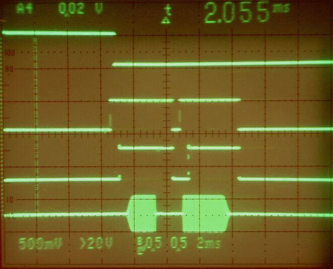
Fig 4. Sequencer waveforms. 1) The keying waveform. 2) PIN diode control. 3) Driver amplifier control. 4) Exciter RF envelope (at IF) |
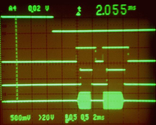
Fig 5. The pilot tone is disconnected. Otherwise identical to figure 4. |
The final amplifier and PIN diode switch.The PIN diodes are run at 1 A each so 2 A in needed in total for the PIN diode switch. The heater voltage for the tube in the final amplifier is a suitable source for a large current like that and has the advantage of not accidentally being unplugged while transmitting. The tube is switched on and off with a switch transistor (at S1 here) In case the DC supply to the PIN diodes fails, the current through the switch transistor will disappear well before the PIN diode current. The final amplifier and PIN diode switch control is very old. It is not safe under all error conditions but it has served well for many years without ever destroying the PIN diodes so I have left it un-changed for now. The logics to build into the PA/PIN combination would be to add a logical AND between "power supply OK", "Current actually flowing through PIN diodes" and "driver amplifier enable" and use it to steer the control grid voltage and the last driver amplifier. |
| To SM 5 BSZ Main Page |