
Fig 1. Some of the component texts are difficult or impossible to read on the PCB. This figure helps to find the tuning capacitors for the local oscillator.
1. Smoke testConnect the coaxial cables from the output of the RXHFA unit to the RX70 unit and make sure that the RX70 is connected to the RX10700 which in turn should be connected to the RX2500, the computer and to the power supply. Do not connect the d-sub connectors to the RXHFA, RX70 or RX10700 units unless you are sure the boxes are properly connected to the computer chassis and the power supply zero. The parallel port interface is an open drain, a 74HC03, and it may be damaged by static electricity. Making sure that ground is connected before the cable to a computer parallel port is connected is always a good idea. Replacing the 74HC03 which is mounted in a socket is trivial, but if the computer parallel port is damaged, repair is not easy.Connect the 9-pin d-sub connectors to the RXHFA, RX70 and RX10700 units to supply DC voltages and connection to the computer parallel port. Look here for details: Controlling WSE units from within Linrad In case the current differs much from the nominal 0.7 A something is wrong. There is not yet any experience on faulty boards so I can not give detailed hints for troubleshooting. 2. Tune the crystal oscillatorIf the board is new and has not been tuned before, set first C147, C148, C163, C165 and C167 for maximum capacitance. See fig. 1 for the component numbering. | |
|
Fig 1. Some of the component texts are difficult or impossible to read on the PCB. This figure helps to find the tuning capacitors for the local oscillator. | |
|
Start Linrad and enter the weak signal CW mode by pressing A.
In case Linrad was already running, you have to exit and re-enter
by pressing X, then B.
This way you clock data into the 74HC174 flip-flops and send
current to one of the oscillator transistors.
Inject a signal with a known frequency into one of the antenna
connectors and set the frequency in the Linrad frequency control
window to a frequency that will make the injected signal visible
once the local oscillator starts running.
First tune the series LC filter until the signal becomes visible.
Set the trimmer somewhere in the middle of the region where the
oscillator runs.
Then turn the frequency adjust trimmer for lower capacitance
until oscillations stop and turn it back to a position where
the oscillations just start.
Go back to the series LC filter and again set it to the center
of the region where oscillations occur.
This time the region is much smaller and one can easily find
the center position.
The series resistance of the resonator which includes the frequency
adjust trimmer increases as the frequency is moved upwards.
At some point the gain of the oscillator in no longer high enough
and oscillations stop.
The series LC filter should be tuned for minimum loss at the crystal
frequency and this tuning becomes sharp if the gain margin is small.
The tuning points are as follows: The series LC filters all load the LO amplifier which has an output impedance of about 3 ohms. The series resonators are all loaded by 3.3 ohm resistors and not only the active filter presents a load to the LO amplifier. If for example the 66.5 MHz resonator is tuned a bit high in frequency it will reduce the open loop gain of the LO at 68.3 MHz to cause the 68.3 MHz crystal to not oscillate as easily. Tune the LO capacitors for all five crystals to oscillate when the LO frequency is set 2 kHz above the nominal frequency. In the first batch of 25 units four crystals had to be replaced because they had series resistances that were too high. Once the correct setting of the series LC filter has been found by the above procedure, tune the frequency adjust trimmer for Linrad to display the correct frequency. If it is not possible to tune to at least 300 Hz below the desired frequency, replace the 0.1uH inductor that is in series with the crystal with a 0.22 uH inductor. Increasing the indictor by 0.12uH will lower the frequency of oscillation by about 800 Hz. In the first batch of 25 units the inductor had to be replaced for five crystals. When tuning several boards it is a good idea to use a pulse generator that emits pulses with a repetition frequency of e.g. 100 kHz. This way a signal will be present every 100 kHz so one does not have to change the signal source settings when switching band. For the testing of the first 25 units a HP8657A set to 200 kHz followed by a heavily saturated bipolar wideband amplifier was used for pulse generator. 3. Balance mixers and tune IF amplifiers and LO buffers.The tuning at both sides of the mixer affect balancing to some extent. There is also some interactions between the LO levels in the two channels because the LO buffers use noiseless feedback and therefore the output load affects the input impedance and how the LO drive power is split between the LO buffer amplifiers.The interaction between the tuning points is not really a problem, the tuning can be done in any order but the procedure described below gives rapid convergency. Each channel has three capacitors at the output which all should be tuned for maximum conversion gain. There is a capacitor and a potentiometer in the mixer that should be tuned for minimum LO leakage with the frequency set to 7 MHz. The LO buffer has an air wound coil that should be squeezed for a similar LO drive level for the 1.8MHz and the 14MHz bands. The first pruduction batch of 25 units was tuned with a 10 dBm two-tone test signal produced from a pair of HP8657A signal generators set for 14.05 and 14.10 MHz. Each generator was amplified in class A power amplifiers and combined in an iron-free hybrid followed by a 6 dB attenuator. The setup was verified to have IM3 below -70 dB at SWR=3. Tuning with a two-tone test signal is not necessary but this way the IM3 characteristics were checked while tuning. A suitable procedure is as follows: Run Linrad in ordinary receive mode to set frequency as described below. Set the gain to 0 dB. 1) Set the frequency to 7 MHz and tune C150 and VR2 for a low LO level at the output connector for channel 1 and tune C152 and VR1 for channel2. Do not send any signal into the antenna connectors. 2) Measure the voltage on each pin of J7 for 1.8MHz and for 14 MHz. The lowest voltage on each frequency should be similar and in the order of 6V. Squeeze L90 for more inductance to increase the LO level for the 14MHz band and separate the turns for lower inductance to increase the LO level for the 1.8 MHz band. Tune L89 the same way for the voltages on J6. Check the voltages on J7 and adjust L90 if needed. 3) Send the test signal into channel 1 and set the frequency to 14 MHz. Tune channel 1 for maximum output signal in the following order: C103, C139, C127, C103, C127. Then tune channel 2: C122, C138, C140, C122, C140. Should any capacitor reach its end position, squeeze the corresponding coil. 4) Remove the test signal and repeat step 1, the mixer balancing After tuning the conversion gain should be -3dB for an output signal of +7dBm for each of the two test tones with IM3 at -40 dBm or below for an IP3 of +30dBm or above. After tuning is complete, set the gain to +5dB and check that the test signals increase by 5 dB and that IM3 increases by about 20 dB. (A 5dB attenuator should restore the +7dBm output with IM3 at -40dBm or below. IM3 does not follow the third order law at these high signal levels.) The noise floorUnder normal operation the noise figure at the input of the RX70 unit is in the order of 15 dB. To get a good visibility for the noise generated by the RXHFA a wideband amplifier with a BFR91A was inserted in front of the RX10700 to give a noise figure of 9.5 dB at the input of the RX70 unit when testing the first 25 RXHFA units. The reason that the amplifier was not inserted in front of the RX70 unit is that the leakage of the LO and all the LO overtones at the IF output of the RXHFA unit would saturate the wideband amplifier. The noise floor of the RXHFA unit is high enough to be well visible with a noise figure of 9.5 dB.Table 1 shows how much the noise floor increases when the output of the 25 first RXHFA units are connected to an amplifier with a system noise figure of 9.5 dB.
Unit          Channel 1                Channel 2
        Gain=0dB    Gain=10dB      Gain=0db  Gain=10dB
          N(dB)       N(dB)         N(dB)      N(dB)
  1       2.9         5.0           3.2        5.3
  2       3.1         5.2           3.0        5.3
  3       2.7         5.1           3.0        5.4
  4       3.0         4.9           3.0        5.0
  5       2.8         4.8           2.9        5.1
  6        -           -             -          - (unit sold)
  7       2.8         5.1           3.2        4.9
  8       2.7         4.9           2.9        5.1
  9       2.7         4.7           3.0        5.2
 10       2.7         5.1           3.0        5.2
 11       2.6         4.8           3.1        5.2
 12       2.7         5.1           3.3        5.5
 13       2.7         4.5           3.0        5.1
 14       2.8         4.8           3.1        5.3
 15       2.8         4.7           3.1        5.3
 16       2.7         4.8           3.1        5.2
 17       2.7         5.1           2.8        5.3
 18       2.8         5.0           3.1        5.6
 19       2.6         4.8           2.9        4.9
 20       2.9         5.4           3.0        5.0
 21       2.8         5.1           3.2        5.5
 22       2.7         4.8           3.1        5.2
 23       3.8         5.5           3.2        4.8
 24       2.7         4.9           3.0        5.2
 25       2.8         5.0           3.0        5.3
Table 1N is the noise level at the output connector of
the RXHFA measured by comparision with a 50 ohm dummy
load. The test system noise figure is 9.5 dB.
G is the gain taken from table 1.
As can be seen from table 1, the noise floor of the RXHFA is typically 3 dB above the noise floor of the measurement system when the RXHFA gain is set to 0dB and 2 dB higher when the RXHFA gain is set to 10 dB. When the RXHFA is used in front of a receiver with 9.5 dB noise figure with the gain set to 0dB, signals are reduced by about 3 dB while the noise grows by about 3 dB which means that the noise figure of the system is 15.5 dB. If the gain is changed to 10 dB, the signals increase by 10 dB while the noise only increases by 2dB so the system noise figure is 7.5 dB. The noise figure of the RXHFA unit itself is typically 13 dB with G set to 0 dB and 6 dB with G set to 10 dB. Close range reciprocal mixing and noise modulationFor this test a low noise crystal oscillator is needed.Run the Delta 44 in its lowest sensitivity mode ("+4dB" with ossmix). Inject a test signal at 14.16 MHz, 1 dB below saturation into the channels one by one. The noise floor at a frequency separation of 5 kHz should not increase by more than 1.2dB in a single channel. The test signal, about 1 dB below saturation with a power level of -10 dBm is at 128.6 dB on the Linrad S-meter. The noise floor with a dummy load at the RXHFA input is at 14.4 dB in 1 kHz bandwidth which means that the system noise figure is 19.8 dB. (The RXHFA unit itself has typically a noise figure of 13dB) At a distance of 5 kHz from the test signal, the noise floor is typically at 15.2 dB. This means that the sideband noise of the local oscillators is at about 9 dB or about -150 dBc/Hz. It only lifts the noise floor from -145.2 dBc/Hz to -144.4 dBc/Hz. This sideband noise is the summed sideband noise of all the local oscillators in the WSE converter chain. In the first production batch of 25 units, a few boards failed this test. One unit gave about 4 dB noise increase in channel 1 but was normal (0.8dB) in channel 2. The source of sideband noise was found to be the input filter. Resoldering the capacitors cured this problem. Another unit had bursts of noise occasionally in channel 2 while channel 1 was normal. The cause was also the filter capacitors in the input filter. One unit had about 10 dB elevated noise in both channels. These problem turned out to be the quality of the soldering of the thin enameled wires of the LO transformers. Heating the soldering points for 5 seconds cured the problem. Wide range reciprocal mixing and noise modulationTo test reciprocal mixing of the RXHFA unit without any influence of sideband noise from the test system, the RX70 -> LNA -> RX10700 -> RX2500 ->Delta44 ->Linrad, a notch filter on 70.040 MHz was used at the RXHFA output. The test signal from a HP608D was run through a crystal notch filter at 14.185MHz and the power level at the RXHFA was adjusted to +15dBm. A low noise amplifier was used between the RX70 and the RX10700. With this setup, a test signal of -27 dBm at 14.185 MHz showed typically 129.0 dB on the Linrad S-meter while the noise floor with a dummy load at the antenna input was typically 26 dB on the Linrad S-meter in 500 Hz bandwidth. The corresponding noise figure is 17 dB. (The notch filter at the output of the RXHFA degrades the noise figure by 1.5 dB due to a small attenuation 145 kHz from the notch)
Unit      Channel 1     Channel 2
           N(dB)           N(dB)
  1        32.7            32.6
  2        30.9            30.6
  3        31.7            32.2
  4        32.3            34.3
  5        36.2            30.7
  7        30.7            34.5
  8        29.9            36.3
  9        35.6            34.6
 10        33.4            33.3
 11        33.1            33.3
 12        31.0            29.8
 13        33.6            31.1
 14        35.8            32.8
 15        35.5            31.7
 16        36.5            36.6
 17        30.9            30.4
 18        29.0            28.8
 19        32.1            32.1
 20        31.5            30.7
 21        35.2            33.9
 22        29.3            34.1
 23        33.6            30.1
 24        30.1            33.8
 25        31.6            31.8
Table 2Reciprocal mixing.
N is the noise level at a frequency separation of 145 kHz
as indicated by the Linrad S-meter in a bandwidth of 500 Hz.
The carrier is at +15 dBm and the zero point of the noise
scale is -198 dBc/Hz.
Table 2 shows that the noise floor is typically at -165 dBc/Hz and that it varies from -172dBc/Hz to -162 dBc/Hz. Such a variation is too large and an indication of a design error. The RXHFA is designed for low sideband noise and it is not acceptable that component variations give rise to such large performance differences. Unit 8 for example shows a very large difference between the channels. Since the RXHFA is a two channel converter it is straight-forward to to compare the individual building blocks of a channel to each other and it was easy to find that the noise is produced in the mixer of channel 2. The reason turned out to be noise modulation by the LO buffer amplifier. The noise originates in the 2905 -5V regulator and replacing it reduced the noise by about 3 dB in channel 2 while channel 1 was not affected. The LO buffer amplifiers are a bit saturated and to what extent noise on the supply voltages produce sideband noise depends on the individual transistor parameters. A reciprocal mixing noise floor at -162 dBz/Hz is certainly perfectly adequate on HF bands, but a modification was implemented on the RXHFA to reduce the consequences of poor filtering of the -5V supply for the LO buffers. To get a good filtering it would have been necessary to insert a small series resistor and an electrolytic capacitor. Cutting tracks is inconvenien so the modification was limited to the addition of a capacitor as shown in figure 2. |
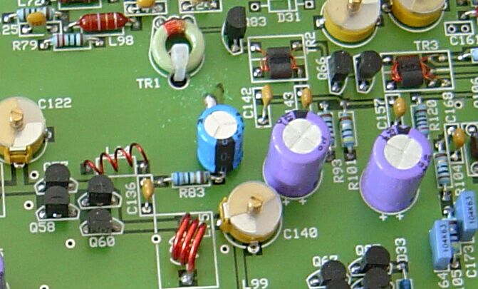
Fig 2. A modification added to the RXHFA to reduce the noise on the -5V line. A 470uF 10V electrolytic capacitor to ground is soldered onto R83. |
|
After adding the electrolytic capacitor as shown in figure 2 most of the units had a noise floor around -170dBc/Hz. A few units had a noise floor that was one or two dB higher than normal, replacing the 7905 helped only in one case. Resoldering the thin enameld wires of the ferrite transformers in the local oscillator as well as in the mixer(s) reduced the noise to normal values. It would probably be possible to reduce the noise floor by 0.5 or 1 dB on most units by heating all soldering points for a long time (10 seconds or so) but it was not done. The noise produced in the joint where the tin meets the wire and the temperature was not high enough for a long enough time to produce good wetting will probably decrease by time when oxides develop on the surface. The noise measured after the modification is shown in table 3. The 7905 was replaced in 4 of the units (but it affected only two of them.) The transformer wires in two of these plus two more units were resoldered.
Unit       Channel 1      Channel 2
             N(dB)         N(dB)
  1        30.4(25.5)    30.2(26.3)
  2        31.0(26.2)    30.5(26.2)
  3        29.8(25.8)    29.9(26.3)
  4        29.8(26.2)    30.2(26.4)
  5        31.2(26.2)    28.9(26.1)
  7        29.9(26.1)    30.7(26.5)
  8        28.9(26.1)    29.7(26.6)
  9        30.5(25.8)    30.2(26.3)
 10        30.6(26.1)    29.6(26.5)
 11        30.0(25.7)    29.8(26.4)
 12        29.3(26.0)    28.7(26.6)
 13        30.1(25.9)    29.3(26.4)
 14        30.9(26.1)    30.0(26.4)
 15        30.5(25.9)    30.3(26.4)
 16        29.3(25.8)    29.8(26.5)
 17        29.7(26.1)    29.2(26.1)
 18        29.1(26.0)    28.7(26.4)
 19        29.9(25.8)    29.8(26.0)
 20        29.8(26.0)    29.9(26.3)
 21        30.3(26.1)    29.1(26.7)
 22        29.0(26.1)    29.4(26.5)
 23        30.2(26.8)    29.0(26.6)
 24        29.4(25.9)    29.7(26.2)
 25        29.8(25.9)    29.6(26.2)
Table 3Reciprocal mixing for modified units.
N is the noise level at a frequency separation of 145 kHz
as indicated by the Linrad S-meter in a bandwidth of 500 Hz.
The carrier is at +15 dBm and the zero point of the noise
scale is -198 dBc/Hz.
The value within parenthesis is the level with no signal and
a dummy load at the antenna input
Typical values from table are 26 dB without and 30dB with signal present. This means that the reciprocal mixing noise typically is at about 27.5 dB on the linrad S-meter or at -170.5 dBc/Hz. The best units are at about -172 dBc/Hz and the worst at about -167 dBc/Hz. The worst units can most probably be improved by resoldering transformers and other components, a few of them become better with a 3000uF capacitor on the -5V line. The variation is still a bit larger than desireable, but in real usage when the sideband noise of the WSE converter chain at about -172 dBc/Hz is added, the sideband noise of the entire signal path will vary less, between -169 dBc/Hz and and -166 dBc/Hz. Second order intermodulationThe first production batch of 25 units was tested with a pair of -10 dBm signals on 7 MHz. The level of the signal at the sum frequency on 14 MHz was checked for each channel and was found to be typically at -108 dBm with the worst unit at -106 dBm. This means that IP2 of the RXHFA is +86 dBm or better. |