During the 27th VHF meeting at nnaboda, Sweden, some measurements was made by SM5BSZ Leif with his high dynamic receiver WSE - Linrad on a 736 owned by the arranger SK4BX. It revealed that the SSB was well behaving, just as I suspected with the RF limiter design of the transceiver, but it also made clear that the CW had some strange modulation. Some investigation made clear that the origin of the interference was the side tone oscillator. The oscillator was isolated from the DC rail by a RC filter and the output was much cleaner.
The rig at my home club SK4AO is also a FT-736R. Some quick tests made clear it had the same problems as the one tested at nnaboda. The schematic diagram was carefully read, and I found the modulator. It is the PIN diode attenuator at the output of TX main unit that has a serious design fault.
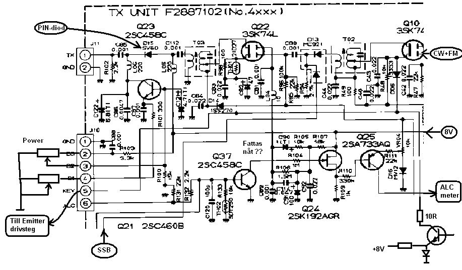
The PIN diode D4015 is placed in series with the signal. When the resistance in the diode is low the output is high, and vice versa. The RF resistance in the diode depends on the current trough the diode. The current is altered by the front panel drive control, a ganged variable resistor/potentiometer connected to a current source coupled transistor, Q4023. One of the resistors act as a variable emitter resistor and the other is changing the base voltage. The current source is well decoupled by capacitors, but here is the fault in the circuit. The decoupling of the collector is made to ground with C4086 and C4122. That apply every noise voltage on the supply voltage directly over the poor little PIN diode. The noise current depends on the noise voltage and the circuit impedance, which is the series circuit of L4005, D4015, L4006 and C4086 paralleled with C4122. The diode do all it can to modulate the signal through it with all that noise. Fortunately, the error is easy to correct.
First, I have to warn you, that the mains supply is right behind and very close to the area where the PIN diode attenuator is located. Pull the mains cord every time you work in that area!
The supply to the PIN diode attenuator goes trough two jumper wires on the circuit board. Cut the first one and solder a 33 ohm resistor to the tabs. Then connect a 220 µF or larger capacitor that can stand 8V or more between the second one and ground. Ground is always relative, especially on single sided circuit boards. In this particular case ground is somewhere between J4011 and T4003. I decided that the T4003 screen can was a good enough ground for the decoupling capacitor, and soldered it there, where our rig also had a ground wire to the 144 MHz unit.
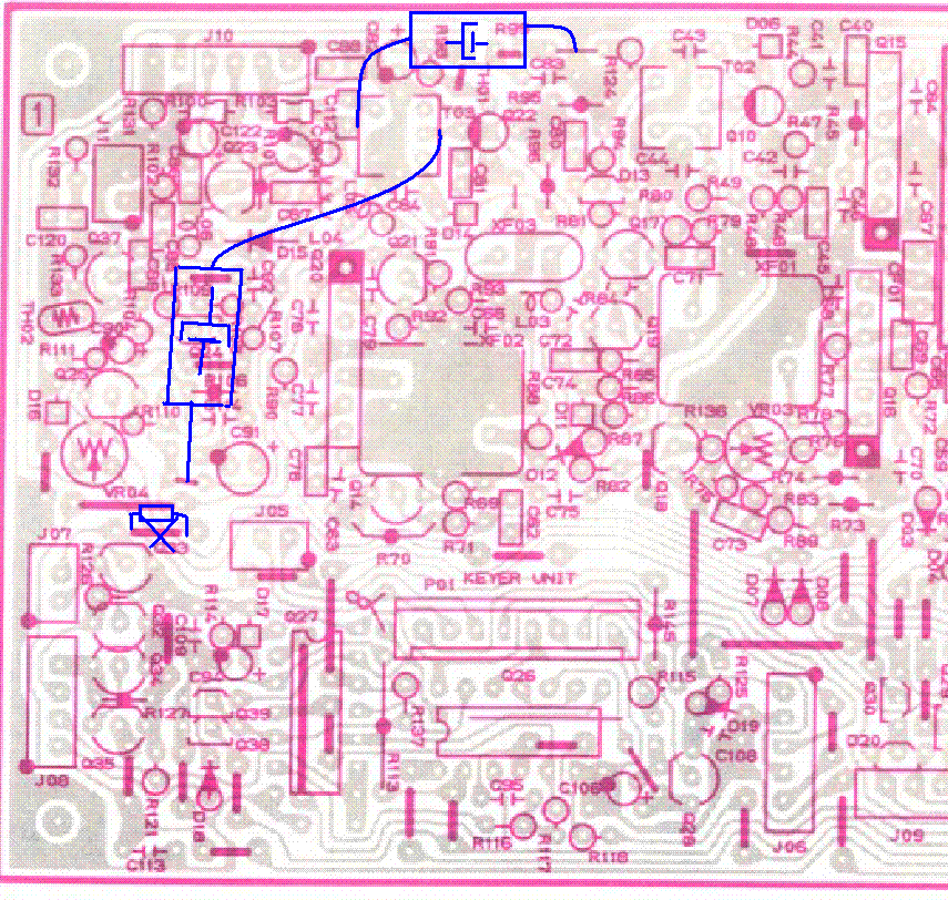
An alternative solution would have been to move the C4086 - C4122 combo to the positive rail instead of ground. But since that involve removing the circuit board, the above solution was chosen instead.
A small adjustment is necessary after the modification. R4107 in the ALC circuit is the only component apart from the PIN diode circuit connected to the now decoupled supply. The voltage is a little lower and VR4004 has to be adjusted a little to keep the ALC meter close to zero. VR4004 affects only the meter circuit, and nothing else.
With the carrier much cleaner, especially at reduced power, now key clicks are obvious. I measured around the circuit board and scratched my head. The schematic diagram and the circuit differ. The keying circuit in the diagram with Q4028 keying transistor seems to be constantly at key down and connected to J4010 pin 5, the keyed stages in the band modules. The keyed stages Q4010 and Q4022 in the TX unit seem to be keyed from somewhere else, but I have not found out from where.
There is a jumper wire right between Q4010 and Q4022 close to the edge where I measured keyed voltage close to 0V at key down and a few volts at key up. I tried a few values of capacitor between the wire and ground and found 100 µF to be a good choice. Here as well I used T4003 can as ground point.
There are still some improvements to be made to the transmitter. The CW signal does not pass any narrow filter, and thus the wideband noise is larger than for SSB. A solution would be to place a filter at the output of TX main unit, the last common place for the TX IF signal before it diverges to the individual band modules. That would also reduce noise in SSB, as one stage less is allowed to transfer noise to the output. The noise at larger offsets would then not depend at all on the drive level.
At low drive levels the noise from the local oscillator and mixer is dominating, at least on 144 MHz. For regular use at low power levels an easy solution is to detune TC6001 and maybe TC6002 in the driver circuit on the 144 MHz main unit. It lowers the gain at 144 MHz, asking for more drive from the IF for the same output. The noise from sources after the PIN diode attenuator is thus lowered as well. This was made on the SK4BX unit and I have done it on the SK4AO unit as well. It is adjusted until there is just a little ALC deflection at full drive.
Before doing anything it is a good idea to tighten the screws holding the circuit boards. They seems to come loose after a while, and maybe also that caused some noise in our unit.
Jan, SM4HFI
Measurements made at Knottebo 2009-06-13
Check with a receiver trough attenuator had already showed that the above changes made improvement in CW, but it was not possible to get any figures from that set-up. I asked Leif SM5BSZ to bring the "golden standard" receiver to the annual VHF meeting at Knottebo, where we made measurements. The measurements was made on the transceiver only, at power level suitable for the 2x 4CX250B power amplifier used at the club.The most stunning result, but not surprising after a deeper look at the circuit diagram, is that CW is over 5 dB noisier than SSB from 20 to about 200 kHz offset, with maximum 8 db difference at 90 kHz. The reason is that the carrier oscillator at 13.79 MHz is passed via just keyed amplifiers, attenuator and LC tund circuits, but SSB is of course passed via narrow crystal filter. I have yet no simple solution to this. The CW transmissions are still in level with many others. SSB transmitter produce a sideband noise lower than any other commercial transceiver measured by Leif SM5BSZ. At small frequency offset this is masked by intermodulation, but still very good. To get the cleanest possible output an external power supply should be used. The internal power supply unit produce a spur with varying frequency offset depending on output power, on our unit 52 kHz at full power and higher frequency when power is reduced. Level is about 10 dB above noise level in 2,4 kHz at full power, in less populated areas it may be acceptable.
I have merged all results I have found from measurements by Leif in a spreadsheet, and added the measurements made at Knottebo of this unit and two others I brought, a TS-790 and IC-260. All three are modified in modulation and/or keying. PLL's and VCO's are untouched.
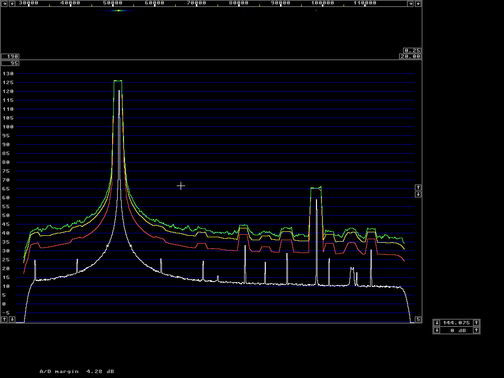
Continous CW spectrum received with the WSE receiver in TX-test mode. This image is the source for sideband noise in the spreadsheet carrier table, spurs are omitted.
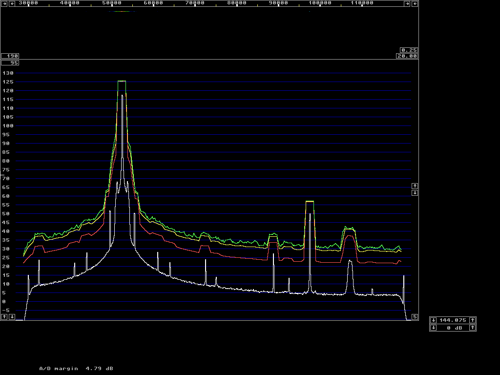
Whistle in SSB spectrum received with the WSE receiver in TX-test mode. This image is the source for sideband noise in the spreadsheet carrier table, spurs are omitted.
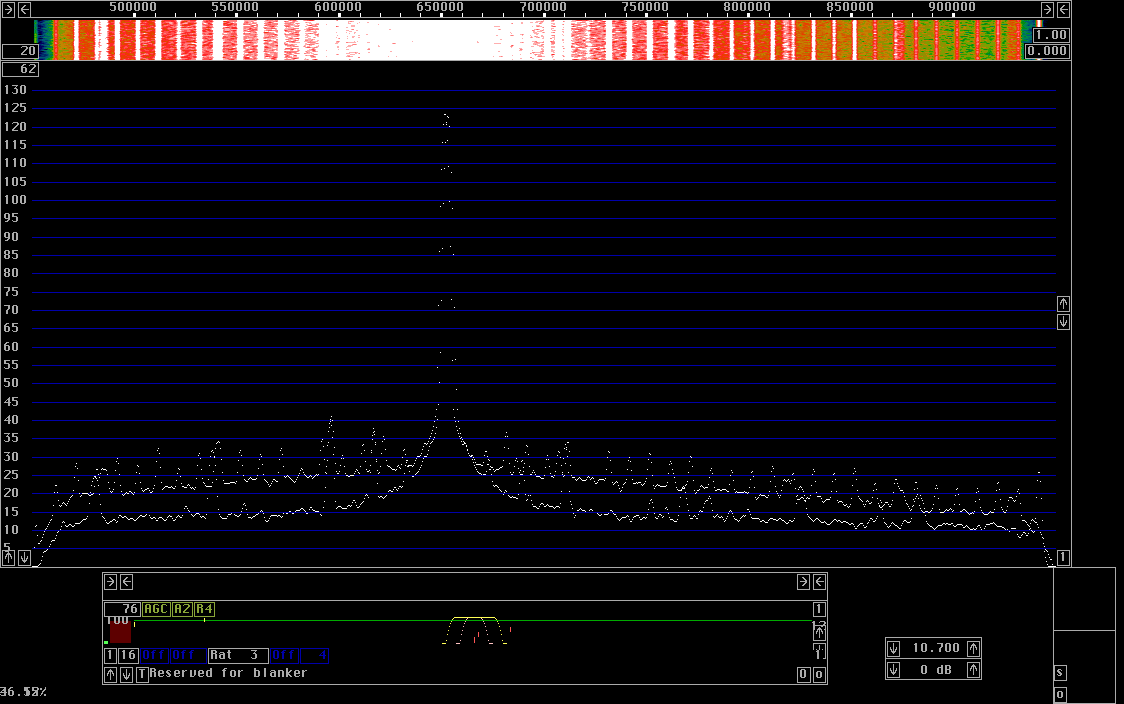
Merged image of whistle in SSB and continuous CW spectrum received with Perseus and WSE converters 144-70-10,7 MHz covering 500 kHz. The SSB output level is 1 dB lower, and at the skirt the lower curve is SSB mode. The CW skirt also have much more spurii. The above mentioned PSU spur can be seen 83 dB below the carrier on one side, slightly better on the other. I am uncertain of the frequency scale direction. The PSU spur level at reduced power was not measured.
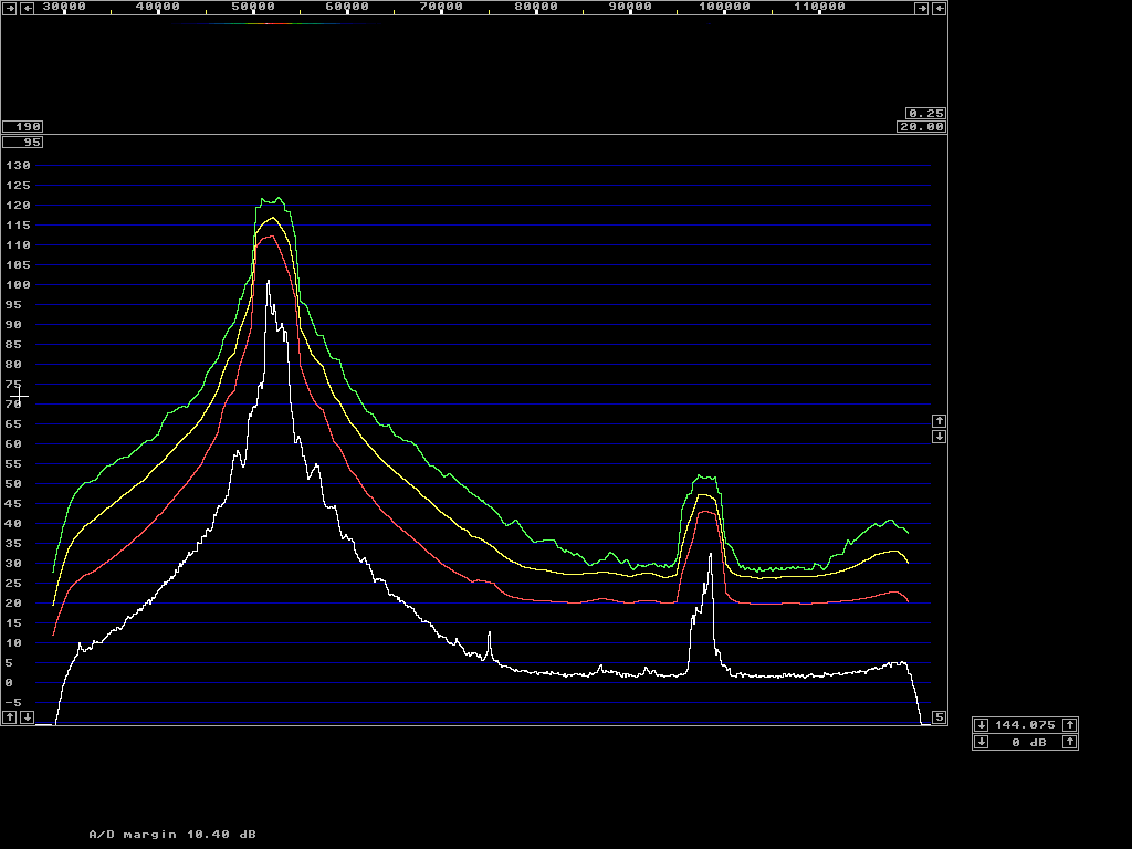
SSB transmission with FT-736 controls as usually set at SK4AO in contest, received by WSE chain and Linrad in TX-test mode. You can compare the power with good accuracy using the A/D marign figure and compare with the figure at full power, Here power is 6 dB down from CW maximum power. The hump at the right edge is propably the PSU spur. The hump at about 100000 is image of the wanted signal in the receiver. This image is the source for sideband noise in the spreadsheet splatter table, the PSU spur and the image are omitted.
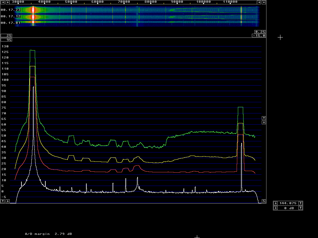
CW mode key down and power altered up and down with internal power supply. Note in the waterfall how the PSU spur frequency varies with power level from 88000 on the scale to the upper scale end.
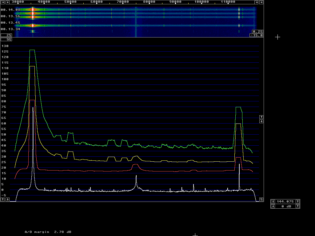
CW mode key down and power altered up and down with battery as power supply. There is no sign of the PSU spur.