Dynamic range of 2 m transceivers Part 5: Modifications to the FT225RD
Published in Radio & Television Nr 6 1981.
Most of this text still in Swedish.
* When we tested the FT225RD we found a rather high level of sideband noise in tx mode and a poor two signal dynamic range in receive mode for the same reason. It also had severe keying clicks and a large bandwidth as SSB transmitter.
* With the modifications described below, the rather poor transceiver is changed to an excellent unit, probably the best on the market.
* It is easy to cure the keying clicks and the excessive bandwidth on SSB transmissions. It is a bit more difficult to reduce the noise sidebands from the VCO. To cure the VCO you need some experience above novice level.
In the previous issue of RT we treated FT221 by Yaesu-Sommerkamp and showed how to lower the sideband noise. Here we discuss the follower FT225RD and explain not only how to reduce the sideband noise but also how to remove keying clicks and splatter in ssb mode.
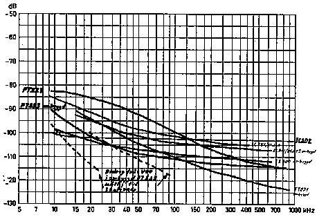
After these modifications have been made, the FT225RD is the best factory built synthesis station we have made measurements on. The noise before and after modifications is shown in fig 1. The figure also shows average values from the modified rigs described earlier in this series. IC202 which uses a VXO is also shown as a comparision.

Fig 1. Sideband noise from FT225RD in transmit mode
before and after modification.
As a comparision some other rigs are also shown in the figure
(coloured in the original article - sorry for the poor image quality).
The comparision curves (with unreadable text at the right side)
are IC202, IC251/IC211(mod), TS700(mod) and FT221(mod).
Note that FT225 is the most noisy station before modifications
at typical CW interference frequency offsets (10 to 50kHz) while
it is the best station of all after modification.
The modifications are tested on two different FT225RD units. The sideband noise is identical between the two units in transmit mode within our accuracy of measurement.
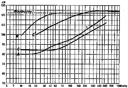
Both units have the original front end replaced by the MuTek board (Kungsimport tel 0300/440 89) The performance of the two FT225RD units differs considerably in receive mode but they are both quite good. The 2-signal dynamic range is shown in fig 2.

Fig 2. Two tone test of the receiver showing how strong
an interfering signal can be (relative to the noise floor)
without reducing the S/N of the desired weak signal with more than 3 dB.
Curve A shows the performance in the original state.
B shows a modified station. C and C' show another station before and
after modification. (The MuTek front end board was used in all these tests)
By comparing fig.1 and fig.2 one can say that the side band noise in transmit mode does not come from the VCO. It must be amplitude or phase modulation introduced by later stages. The contribution to the tx noise that comes from the VCO is indicated by dotted lines in fig1. One of the stations, B in fig.2 has extremely low VCO noise. Very probably the wide band tx noise can be reduced by 15dB by simple means, which would make the transmitter equally good as the receiver.
Common error causes sideband noise
The modification required to reduce the sideband noise is exactly the same as the one needed for IC211/245. The error in the VCO is the usual one, the capacitance diode is fed through a resistor instead of an inductor. The resistor creates noise that modulates the VCO signal. This FM modulation is the noise sidebands.Unfortunately the electrically simple change is a bit tricky from a practical point of view since the VCO board has to be desoldered from its motherboard (pll-unit). Some skill in desoldering is required. Watch out for the three pins with +8V, control voltage and RF out to be completely desoldered from the motherboard before you try to remove the VCO! The pins are not well secured to the VCO board, and they are easily pulled out together with parts of the copper conductors of the VCO board.
The modification is to replace R1001, a 100 kohm resistor, with a rf choke. R1001 is located between TC1001 and the two capacitance diodes. It is very important that the choke is mechanically well attached to the board. Vibrations cause FM modulation which the (after modifications) slow PLL will not cope with. You may solder the grounded end to the ground plate on the top side of the VCO board.
Choosing a good rf choke
We have received several letters with questions about what inductor to choose in the modifications for IC245/211 and FT221 Below is some more information about what the rf choke and its operation. It is valid for PLL loops in all transceivers, not only at VHF.The choke has to pass DC voltages and audio frequency AC voltages to the capacitance diode(s). The choke forms a low pass filter with the capacitance diodes and possibly other capacitances that from an audio frequency point of wiev is in parallel. This low pass filter has to produce a small phase shift at the highest frequency for which the phase locked loop gain is above unity. Practically a 3dB point of 5kHz may be ok which means that the choke may be up to 100H or so. In other words, there is no upper limit for the inductance.
The choke is in parallel with the resonance circuit. The important thing is that it does not degrade the Q. At VHF a single layer inductor wound on a ferrite rod combines high inductance and low capacitance to form a very high impedance that does not add losses to the resonat circuit. It does not change the resonant frequency much either.
In our modifications of 2 m-transceivers we have used RF chokes from TV-tuners. They are wound by about 30 turns on a 12mm long ferrite rod with about 1.5mm diameter. The inductance is about 10 microhenry.
When you glue the inductor to the board to make it mechanically stable, make sure that you do not create a large and lossy capacitor between the hot ent of the inductor and ground. In other words, make sure the glue layer is thick or use some insulating spacer to make the stray capacitance small - and thereby its losses.
The noise from the loop is reduced by a filter
For FT225RD as for IC211/245 it is nessecary to add an extra filter in series with the control voltage for the VCO. This filter is shown in fig.5 in the article about IC211/IC245.The 33 kiloohm resistor can be placed between the feed thru capacitor C1049 and the motherboard. The other components are conveniently placed on the back side of the motherboard.
When the modifications are done to the FT225RD it is not nessecary to perform any adjustments provided the RF choke did not change the resonant frequency to much of the oscillator. If the frequency has to be adjusted, change TC1001 until the voltage at C1049 becomes 3V when the transceiver is tuned at 144.000MHz.
A further improvement is possible
We have done some experiments in order to further lower the sideband noise from the VCO in FT225 by making the coupling between the transistor and the resonant circuit looser. This was sucessful in one of the units while the oscillator stopped oscillating in the other. Consequently the unit C in fig 2 has only the modifications described above.In station B the LC circuit of the oscillator was looser coupled to the transistor by changing of C1005 from 7 to 4.7 pF and by changing C1006 from 3 to 10 pF. (In the schematic diagram C1006 has some other value)
At a frequency separation of 20 kHz the sideband noise is improved by about 2 dB by the looser coupling of the oscillator in station B. We decided that this improvement is insignificant and did not try to optimise or to try to find out why it did not work in station C since we were experimenting with the rig in transmit mode as usual. Afterwords we have found that the sideband noise of the VCO itself does not contribute much to the transmit noise at this frequency separation. It is therefore possible that changing these capacitors improves the receiver by far more than 2 dB, which is indeed the case as shown below.
Afterwards (when we no longer have access to the rigs) we can see that the noise decreases by more than 9 dB going from 10 to 20kHz frequency separation in receive mode. This shows that part of the VCO noise comes from the voltage that controls the frequency through the capacitance diode. It should be possible to get another 5 dB or more at 10kHz frequency separation by increasing the resistor that (after the modification) is located between C1049 and the VCO to 100 kohm. In order to avoid excessive lock times the resistor should be connected in parallel with two crossed diodes (1N4148 or similar). There may be some complications which we will not discuss here.
A poor transceiver converted to a top class unit.
It is uncertain whether it is possible to devise a reproducible modification scheme that will make all FT 225 transceivers as extremely good as the station B in receive mode. We think it may be valuable to make the mods available already now since it is quite clear that the FT225 after modifications is superiour to its competitors and that it is possible that it can become even far better. Consider this information when you decide what rig to buy, but do not forget the important modifications. If you use the FT225 in original shape you will cause interference to your fellow amateurs by your transmissions and you will experience avoidable interference in receive mode.
Keying clicks, noise and ssb splatter.
This series of articles is inspired by the large scale test of two meter transceivers that was published in RT 1980 no 3. Besides excessive sideband noise we found that some stations create severe keying clicks - a phenomenon that many two meter operators have obvious experiences of. We also found that the bandwidth of the ssb transmit signal was too large, although not disastrously.After having treated the sideband noise in four transceiver types it could be appropriate to treat keying clicks and ssb splatter. In the large scale test FT225RD was the worst rig in ssb mode causing quite a lot of splatter. It also has severe keying clicks, so this station is a good candidate to demonstrate how to proceed.
It is easy to remove keying clicks completely.
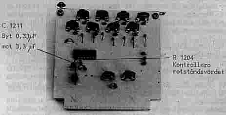
It is quite simple to make the keying perfect in FT225RD. In the keying circuitry there is a pulse shaper, Q1201. It is followed by a low pass filter R1204 and C1211. C1211 is loaded by R1205 which goes to the base of the keying transistor Q1202. In the original shape the keying clicks spread out over +/-20 kHz.By replacing C1211, a 0.33 microfarad capacitor by an electrolytic capacitor of 3.3 microfarad (see fig 3) one gets a suitable time constant. The fall time is about 2 milliseconds at the antenna connector. The rise time is shorter. In one of the rigs we adjusted it by connecting a 27 kiloohm in parallel with C1211.
In the other station R1204 was only 10 kiloohm (the schematics show 47 kiloohms). That rig gave equal rise and fall times with R1204 = 33 kiloohm without any resistor in parallel with C1211
After the mods the rise and fall times are 2 milliseconds in both the rigs.
For perfect keying one more modification is required: The signal from the collector of the keying transistor is keying the transmitter in two ways. Firstly it goes to the emitters of two of the transmit amplifier stages. Secondly it goes to the source of Q510, a power regulating transistor. The voltage swing required to control Q510 is much smaller than what is needed to control the emitters.
A voltage divider is required to reduce the amplitude of the keying signal at the source of Q510. Without this voltage divider one gets dual time constants in the output signal.
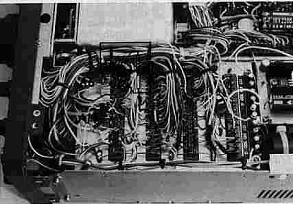
By use of three resistors one gets perfect keying. The resistors are placed on the connector J22 (mic amp unit PCB connector). See the photo, fig 4. Note that the numbering on the connector does not agree with the numbering in the circuit diagram!
Here is a step by step description:
Remove the wire that connects B3 to B6. (B3 on the PCB connector is numbered 6 in the circuit diagram and B6 is numbered 12.)
(2) Move the remaining wire from B3 to B6.
(3) Solder a 6.8 kiloohm resistor from B6 to B3.
(4) Solder a 1.8 kiloohm resistor from B3 to B1 (ground).
(5) Solder a 1 kiloohm resistor from B6 to A3(+8V). (A3 is numbered 5 in the circuit diagram).
With the modifications described above the keying speed is limited. The rise and fall times of 2 milliseconds should allow around 1000 letters per minute, but the time delay in the keying circuitry is large and makes the maximum speed much lower. We will come back to that in a later article.

Fig 3. "Cw keying unit (PB-1721)" is
the name of the board in this figure.
A resistor may be connected in parallel to C1211 on the
other side of the board.
That resistor and R1204 determine the rise time, see the text.
The fall time is determined by C1211 and R1205.
Peak power versus average power in ssb
The simple and cheap modifications we have described sofar in this series of articles are uncontroversial and we hope the manufacturers will incorporate these in their future production!For the FT225 RD only one wire has to be moved in order to eliminate completely the splatter in ssb mode. This way of curing ssb splatter is however not entirely uncontroversial but it is of fundamental interest. For that reason here is first a short general discussion about ssb.
When designing a ssb transmitter for amateur use two entirely different starting points are possible:
1. The transmitter shall give the best possible readability for weak signals but the DC input power to the power amplifier must never exceed a certain average level and it shall be measured with an instrument having a time constant of 0.25 seconds.
2. The transmitter shall give the best possible readability for weak signals but the power amplifier has limiting power level and can never produce more than a certain maximum power.
We start by investigating how an optimum transmitter should be designed according to point 1: (Legal limit criterion in SM 1981)
The transmitter shall be completely linear in amplitude and the bandwidth shall be the same as the bandwidth used in the receiver, i.e. around 2 kHz. When one says "aaaaaaaaa..." in the microphone of such a transmitter the peak power is about 12 dB higher than the average power. With normal speech input, the ratio between peak and average power is at least 5 dB higher. All measured with 0.25 seconds time constant.
If we assume that the power amplifier can be operated linearly without any noticeable zero power (which is possible by use of certain tricks) an amateur with a C licence and a maximum permitted power of 10W would need a power amplifier that momentarily uses 500W input power. The average power measured by a 0.25 seconds time constant would still stay below 10W.
Wi may now compare with the second starting point above. Assume that the power amplifier saturates at 10W. If such a transmitter is driven entirely linearly the average power becomes only 0.2W. The peak power will only be transmitted in the peaks of the voice signal. The letter a (my voice) for example gives pulses with a length of 2 ms separated by 30 ms and is particularly difficult. If one cuts the amplitude to one third (voltage) it is impossible to hear any difference in voice quality, regardless if the amplitude limiting is performed in the AF or in the RF section of the transmitter. Splatter may of course be produced if the limiting is done improperly.
The readability is not affected by this limiting even though the peak level of the received audio signal is reduced by 10 dB because the average power is unaffected. (It is assumed that the limiting process changes the gain slightly to keep the average power constant.)
When the peak power is reduced by 10 dB one can obviously increase the average power by 10 dB to 2W, still without saturation at the 10W maximum level for the power amplifier. The result is 10 dB better signal strength. It is quite ok to use harder limiting, but when very hard limiting is used it matters slightly how the limiting is performed, and then a RF clipper is superiour.
A two tone test is misleading.
Many articles have been written on the advantages of RF clippers compared to audio clippers. Usually these articles show how a sine wave or possibly how two equally strong sine waves are affected by RF and AF clipping respectively. That is directly misleading at modest clipping levels because the human voice is very far from a sine wave or two! Audio clipping is not often used on purpose in amateur transceivers, probably because of the undeserved bad reputation. In FT225 RD the alc circuitry is used to produce a clipping function instead. This is very ugly and the reason why this transceiver produces a lot of splatter in its original shape! har splatter! If the microphone gain control of a FT225 is set for the instrument to show half scale (average power 6 dB below full power), the alc circuitry has to reduce the gain of the transmitter by 10dB to avoid limiting in the final transistors. This gain reduction has to be done to a large extent after the filter, otherwise it acts to slowly. Changing the gain is amplitude modulation. There are no low pass filters in the alc cirquitry so the amplitude modulation contains frequencies up to 100kHz or so and consequently the splatter extends about 100kHz on both sides of the signal.The clipper circuit is already in place in FT225!
The cure for the splatter is to feed the ssb generator with the beautifully limited and filtered audio signal that is normally used for the FM modulator.At long distances it is completely impossible to decide whether the clipping is done at AF or by the alc circuitry. The amateurs living nearby will however note a dramatic difference.
The splatter is completely absent even if the ssb power is set at 75 % of the CW power. How the speech quality is affected by the clipper can be checked by listening to the station in FM mode.
The modification is simple: Just move one wire.
As already mentioned, this modification is extremely simple. Move the wire from pin 14A to pin 6A on the PCB connector J22 (mic amp unit). See the phot in fig 4! With the numbering of the schematic diagram the wire should be moved from pin 27 to pin 11.Once the wire is moved, the ssb peak power is controlled by "ssb mic gain" at the front panel. The average power, i.e. the clipping level is adjusted by VR501 in "mic amp unit". After the modification VR501 will affect both the FM and the SSB transmissions.
To set the peak power "ssb mic gain", feed a sine wave (whistle in the
microphone) in the way that produces maximum power. Adjust for the
power to be 10 % below maximum power.
Then set VR501 for the power meter to show half that reading when you say
"aaaa..." in the microphone - with normal voice and at the normal
microphone position.

Fig 4. The AF clipper is inserted by disconnecting the wire that
goes to the pin A14 and moving it to the pin B6.
Then follow the step by step description about keying.
Nearby amateurs no longer a problem.
Finally we want to point out that FT225RD to our knowledge is the first factory made transceiver that may allow two amateurs to live as close as 500 meters from each other and use 300W output power (Remark: maximum allowed in Sweden in 1981) without causing interference to each other at a frequency separation of 50kHz and with parallel antennas. - During band openings one usually wants to work in the same directions.The worst case is when the main lobe of one operator points straight into the back lobe of the others antenna. 10 element antennas with 20 dB front to back are assumed. (Compare to table 1 page 11 in RT 1980 no 3.)
This requires the looser coupling between the resonant circuit and the transistor in the VCO is sucessful. It will also be nessecary to lower the wideband noise in the transmitter by about 15dB, which is probably not difficult.