The series resonance oscillatorA 10 MHz crystal is typically 4 ohms at its series resonance and 40 kiloohms at its parallell resonance. To get low sideband noise the power dissipated in the crystal has to be reasonably large, the design used here dissipates 0.2mW in the crystal, 7mA and 30mV across the crystal.An oscillator can be seen as an amplifier which has feedback through a filter. The amplifier of a series resonance oscillator must have both a low input impedance and a low output impedance, preferrably below 4 ohms to preserve the selectivity associated with the high Q of the crystal. The thermal noise in the losses of the crystal is k * T0 = -174 dBm/Hz. With a power dissipation of - 7 dBm the flat noise floor is thus 167 dB below the carrier if we compare the power dissipated in the losses of the quarts to the thermal noise generated by the same losses. The flat noise floor at the collector side may be a good deal better than this even if the amplifier impedance is matched to, or lower than the resistive part of the crystal impedance. This is because the voltage gain for the thermal noise produced within the crystal drops quickly with the frequency separation since the reactive part of the crystal impedance comes in series with the noisy 4 ohm resistive part. The noise generated by the transistor itself will be attenuated by the large emitter impedance presented to the emitter by the crystal at frequency separations of a few kHz or more so the flat noise floor may be well below 167 dBc/Hz. The flat noise floor can be made much lower than one would expect from comparing noise power to signal power using the noise figure and feed impedance at the resonance frequency of the crystal. A termination resistor from emitter to ground may improve the noise close to the carrier but it may degrade the noise floor by more than 10dB at large frequency separations.
The parallel resonance oscillatorEverything is inverted. With the same power dissipated in the crystal and the same temperature one gets the same result for an ideal amplifier. Here the noise voltage generated by the losses in the crystal is shunted by the much lower reactive impedance of the crystal far from the resonance.The parallel resonance oscillator needs an amplifier with an input impedance of at least 40 kiloohms. To give a good performance close to the carrier, the noise figure has to be low at 40 kiloohms input impedance. To give a low value for the flat noise floor far away from the carrier, the amplifier has to have a low noise figure also at source impedances below 1 kiloohm. My personal experience with parallel resonance oscillators is not as good as with series resonance ones, that is the reason a series resonance oscillator was chosen as the pure oscillator required in the 2.5MHz high performance direct conversion receiver.
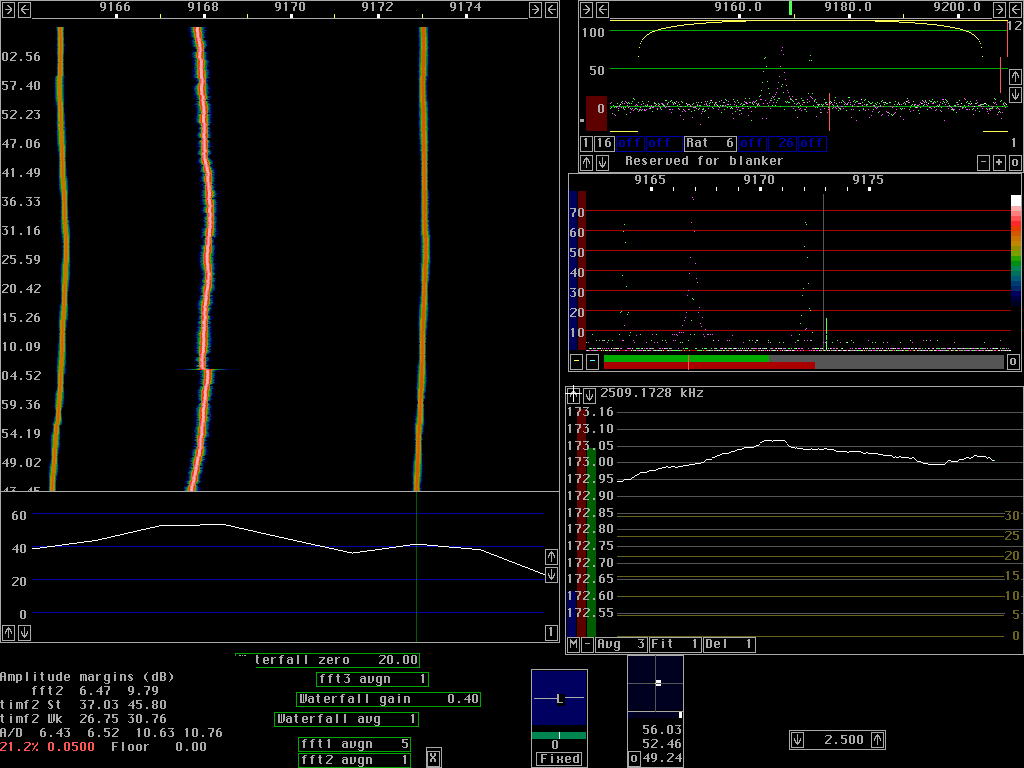
Practical details of the series resonance oscillatorThe oscillator has the crystal in series with the emitter of a bipolar transistor. The complete circuit diagram is shown in fig. 1. The input impedance of a grounded base BF240 is about 4 ohms if the transistor is run in class A.The impedance across 4.7nF is about 3 ohms. Feedback is through 100 ohms of capacitive reactance and 10 ohms of resistive to get feedback in the correct phase. The 10 ohm resistor is also a load for the output of the amplifier, it dissipates about 30mW of LO power. The design presented here runs the BF240 transistor in class C which results in a very poor performance close to the carrier. On the other hand, the flat noise floor far from the carrier is very low. See for example the article by Gerhard Hoffmann, DK4XP in Dubus 2/2001 The flicker noise close to the carrier could be reduced by use of a more complex oscillator design but that would only affect performance closer to the carrier than about 1kHz. It would of course improve short time stability also. In my experience, running oscillators in class C may improve the flat noise floor far away from the carrier. At a carrier frequency of 2.5 MHz, far away means 10 kHz or less. It seems that saturating the transistor at the carrier frequency will reduce the gain and therefore the noise at frequencies far away. Saturation may also cause some phase modulation that degrades the performance close to the carrier. Class C is good at low frequencies but a bad idea for VHF oscillators, particularly if they are intended to be used to generate microwave frequencies. Here is some information about state of the art VHF crystal oscillators This oscillator is choosen to give a very low level of reciprocal mixing for signals just outside the visible passband at frequency separations in the range 10 to 100kHz. At larger frequency separations, reciprocal mixing is not present because the RF filters will prevent strong signals more than about 50 kHz outside the visible region.
|
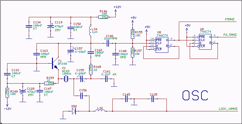
Tuning of the oscillator is finding the position of the collector capacitor which makes the oscillator run with a small value of the series (frequency tuning) capacitor. When the series capacitor is very small the Q of the crystal plus series capacitor is degraded and at some point the gain is not high enough to overcome the losses so oscillations stop. The collector capacitor is this way set for maximum gain.
The inductor in the collector is made small enough to allow 150pF for feedback, 82 pf very close to the transistor to avoid VHF oscillations, 20pF for the load and 30pF for the tuning capacitor. The inductor value that fits is 1 microhenry.
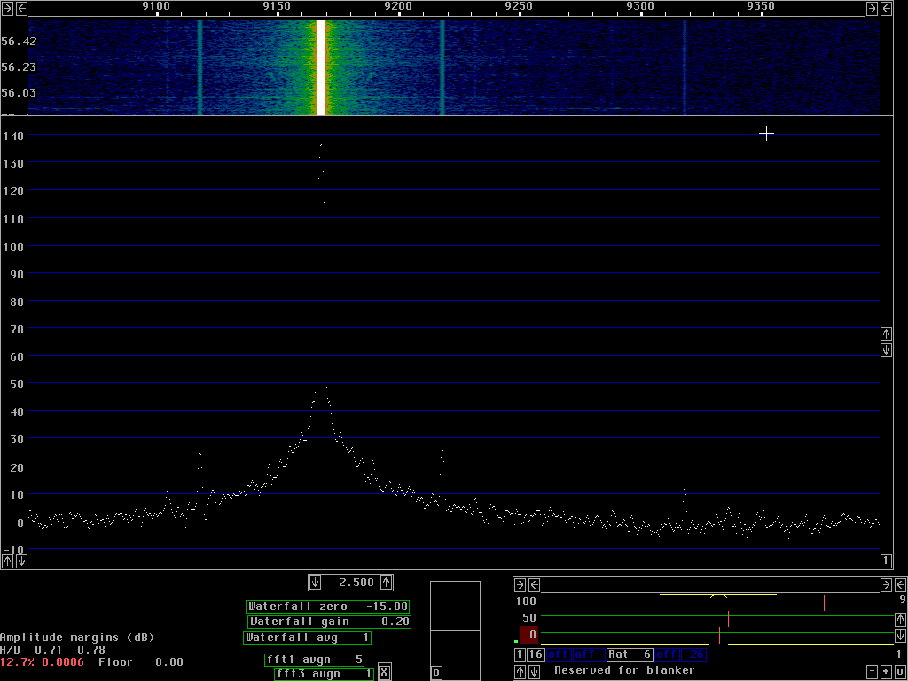
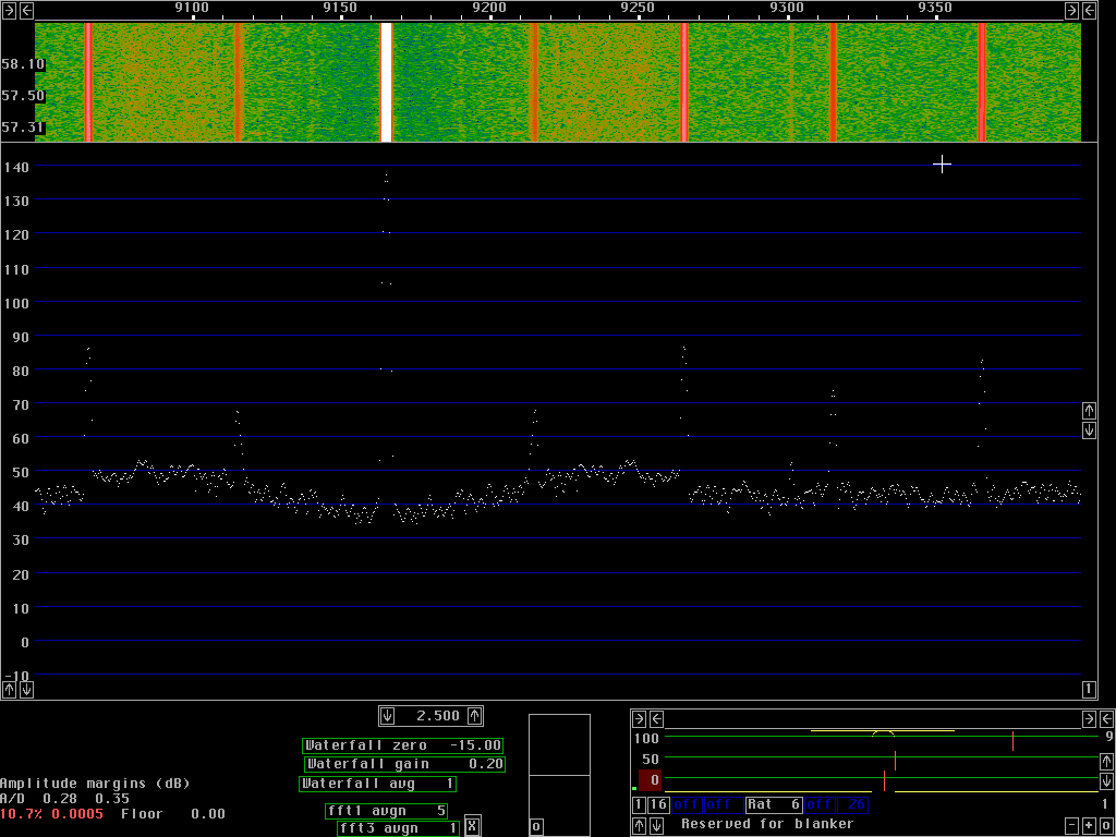
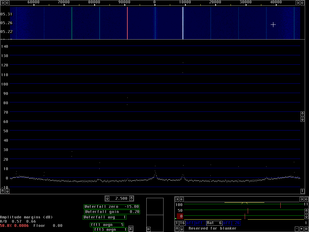
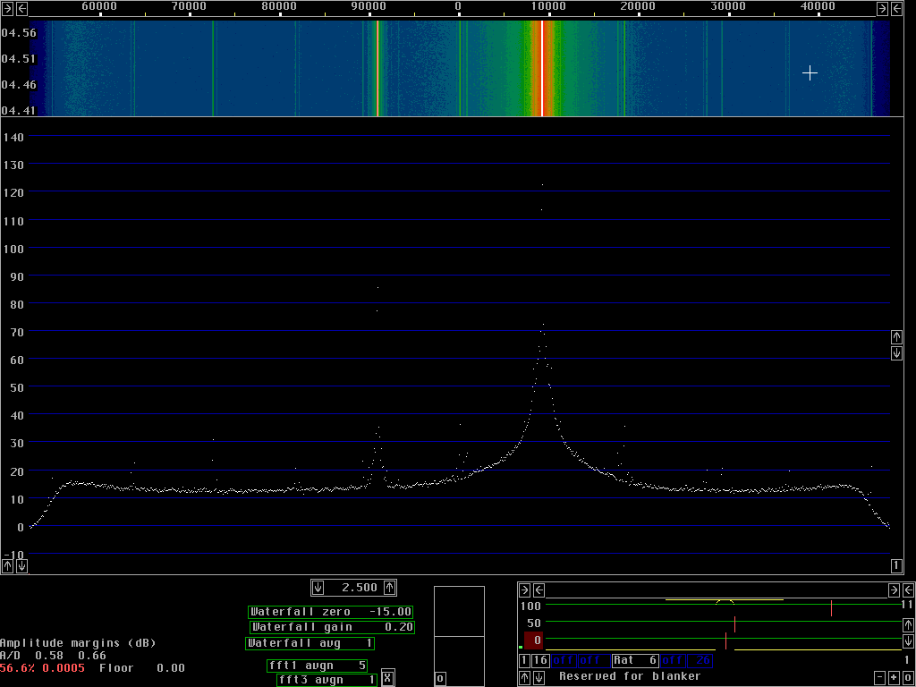
Whether the sideband noise is at -138dBc/Hz or at -93dBc/Hz at a frequency separation of 100Hz does not matter for the practical usefullness of a radio receiver. It is quite another thing what happens at a few kHz frequency separation and above. A local oscillator must have very good sideband noise to avoid receiver desenzitation due to reciprocal mixing. Figures 4 and 5 show the class C test oscillator and the HP8657A in a 90 kHz wide frequency band with a filter bandwidth of about 6 Hz. Since the bandwidth is 6Hz and the pixel separation is about 90 Hz one can not read the signal levels from the screen in these images. The minimum noise floor in fig. 4 at 2.485kHz is at -146.5 dBc/Hz which means that dBc/Hz for the noise floor in figures 4 and 5 can be obtained as the scale reading - 142dBc/Hz.
The purpose of fig. 4 and fig. 5 is to give a hint to why the rather complicated solution with many converters has been choosen for the Linrad hardware. Even a good general purpose syntesised signal generator like the HP8657A is far from adequate as a receiver local oscillator.
Provision is made to lock the LO to a reference should better long term stability be desired. To get the frequency stability demonstrated above the temperature variations have to be kept well below 1 degree and the unit must have been running for a few hours.
